Functional materials and sensors
The growing need for sensors accompanies the progress of various techniques for the development of nanomaterials or nano-architected materials based on dielectrics, semiconductors and/or hybrid materials. In this context, the main activities of the Functional Materials and Sensors theme of our team are part of the study of (i) plasmonic nanosensors for the detection of gases or pollutants, (ii) plasmonic sensors based on semiconductor nanoparticles and (iii) chemical sensors based on organic field effect transistors (OFETs). In general, the sensors developed by the team target applications in the fields of energy, health and environment.
Developed topics
Plasmonic nano-sensors for gas detection
|
Persons involved: Nicolas Javahiraly, François Le-Normand, Nacer Boubiche
|
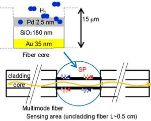
Hydrogen is presented as the sustainable energy vector of the future, because the hydrogen cycle is one of the most ecological among energy solutions. Hydrogen can be used to produce, store and transport energy and its possible applications are very varied.
However, the use of hydrogen presents a significant risk if it is not controlled because it is explosive at 4% in the air, hence the current need for the development of hydrogen leakage nano-sensors for security issues.
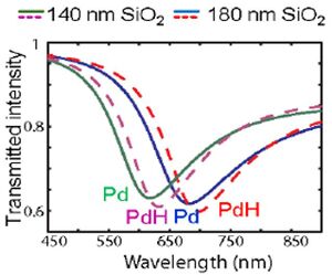
This group activity is devoted to the search for innovative optical hydrogen leakage sensors exploiting the properties of MIM (Metal Insulator Metal) structures, original nanoparticles (simple NPs, core-shell systems, etc.) and their effects (SPR and LSPR ), to bring real progress in detection performance, for example in terms of sensitivity and response time (ANR NHYLEDECT (lead: Nicolas Javahiraly) in collaboration with the University of Lyon 1).
Micro-pollutant plasmonic sensors
|
Persons involved: Nicolas Javahiraly, François Le-Normand
|
The detection of micro pollutants by original systems constitutes one of the important challenges of our society. The cancer agency of the WHO (World Health Organization) has classified five pesticides as "possible" or "probable" carcinogens for humans. This activity of the MACEPV group is dedicated to the study of innovative pollutant sensors exploiting the interaction properties between light and original nanostructured materials. The detection is based on the variation of the, for example, optical properties of the materials used in the presence of the molecule to be detected. Several avenues of investigation are being studied: detection by Surface Plasmon Resonance (SPR) or Local Surface Plasmon Resonance (LSPR) and secondly, that using carbonized structures (Diamond-Like Carbon - DLC)) functionalized but also those exploiting the effects of variations of different parameters (conductivity, resistivity, etc.).
Plasmonic biosensors based on semiconductor nanoparticles
|
Persons involved: G. Ferblantier, E. Steveler, D. Muller
|
Semiconductor nanoparticles (Nps-SC), especially of silicon, integrated in a dielectric matrix, have aroused great interest in recent decades because of their many possible applications in optoelectronics (IR photonic conversion, heterojunction photovoltaic cells, efficient absorbers). In recent years, electrically doped Nps-SCs have attracted a lot of attention because of the possibility of obtaining localized surface plasmon resonances (LSPRs) whose position can be adjusted according to the amount of free carriers in the particles. This adjustment, which is impossible for metallic nanoparticles, represents a major advance in the use of LSPRs in the field of sensors.
Currently, one of the team's activities is to explore the possibility of using these hyperdoped semiconductor nanoparticles (fabricated by sputtering, PECVD or ion implantation) to generate surface electron waves, i.e., surface plasmons, to detect chemical and/or biological agents by modifying the localized plasmon wave.
Chemical Sensors OFETs
|
Persons involved: Yves-Andre Chapuis, Patrick Lévêque, Thomas Heiser |
Chemical sensors based on organic field effect transistors (OFETs) are currently facing a number of technological challenges such as improving sensitivity, selectivity, ambient stability and manufacturing costs. In ICube's MaCEPV team, we are exploring the performance of different types of organic semiconductor (OSC) based materials in the detection of gas species through morphology control and molecular engineering. For example, we are exploiting materials based on "one-dimensional (1D) monocrystalline nanowires" [1], which offer the prospect of faster and more accurate response and recovery rates for chemical detection. In parallel to this work, critical factors from gas kinetics to sensor-analyte interaction, as well as the examination of detection mechanisms are addressed. We are also interested in applications of flexible sensors that can be integrated into skin or clothing.
[1] : ANR Transfilsen (2009-2013), « Transfilsen: Elaboration of transistors based on functionalized and insulated molecular wires and applications in chemical sensors »
Quantum sensors
|
Persons involved: D. Muller
|
The "Double Electron Electron Resonance" (DEER), allows the measurement of the magnetic dipole coupling between 2 electron spins using pump-probe magnetic resonance experiments with two different microwave frequencies. Associated with spins of the colored centers obtained by ion implantation (for example the NV center of diamond), this technique allows the detection of a small number of qubits, or even a single spin qubit.
We plan to develop this technique (OD-DEER by optical detection of photoluminescence) in order to reach sensitivities of a single spin probe which could eventually have important biomedical applications. However, to achieve such ultimate sensitivity, the DEER methods must be combined with a quantum sensor having one or more optically detectable colored centers near the surface. We are working on developing by ion implantation such colored centers with adequate localization and especially maintaining a sufficient coherence time (qq 10µs) at room temperature.


