News
Thursday 21 of March at 10:00, room 25 of building 40 (campus Cronenbourg) |
"Electronic Structure Properties on Inhomogeneous Photocatalyst Systems" by Professor Mitsutake OSHIKIRI of National Institute for Materials Science (NIMS), Layered Nanochemistry Group, Nanomaterials Field, Research Center for Materials Nanoarchitectonics (MANA), Tsukuba, JAPAN
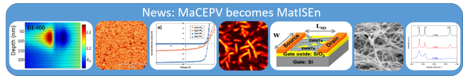
MaCEPV changes name to MatISEn for Materials for Information technology, Sensing and Energy conversion |
Friday 7 of july 2023 at 2:00 PM, amphitheater Grünewald (IPHC, building 25 of campus Cronenbourg) |
HDR defense "From spin coherence and ODMR in semiconductors to SiC-YIG quantum sensors and quantum processors" by Jérôme Tribollet
Friday 30 of june 2023 at 9:00 AM, amphitheater Grünewald (IPHC, building 25 of campus Cronenbourg) |
"New strategies to improve the transparency of photovoltaic optical modulators for smart windows" by Yuhan Zhong
|
Title : Chalcogenide and oxysulfide perovskites for optoelectronic
and photovoltaic applications
Link to the detailed thesis subject in English
Contact : T. Fix at tfix AT unistra.fr
Applications are closed.
Wednesday 17th of May 2023 at 9:00 AM, room 20 of building 40 (campus of Cronenbourg) |
" Tunable plasmonic Rectennas to produce electricity by exploiting the wave nature of light " by Anil Bharwal
Wednesday 29th of March 2023 at 10:00 AM, Auditorium of IPCM (campus of Cronenbourg) |
" Quantum photonics and optomechanics in nanostructures "
The mornings of Thursday 30 and Friday 31 March 2023, by videoconference |
"Organic Electronics: “From component to applications” " by the EEA club
Monday, March 27, 2023 from 9:30 a.m., Location to be confirmed |
"Modeling approaches for the IMEE axis" by Y. Hoarau, S. Leclerc and J.-M. Dischler (ICube)
Program and summaries of presentations
Wednesday 15 of march 2023 at 10:00 am, ICS amphitheater Henri Benoit (Campus of Cronenbourg) |
"New advances in tetrazines and heptazines chemistry. Fluorescence, photocatalysis, and applications to organic photovoltaic" by Pierre Audebert
Abstract :
s-Tetrazines, and the far more enigmatic heptazines, which count much less described examples, are among the most electron deficient high-nitrogen content, stable aromatic heterocycles (Fig. 1). This peculiarity confers them very original physico-chemical characteristics, including delayed fluorescence, a high electrochemical reduction potential, and a strong potential in organic photocatalysis. In
addition, heptazines can trigger enhanced electron transport in OPV devices. However, their synthetic approach, for heptazines, is still in its infancy. We will present and comment on new strategic synthetic procedures involving these two families, insisting more on heptazines recent results, and new properties.
This lecture will therefore recall new synthetic advances in both fields of tetrazines, and heptazines. Noticeably, a new synthetic procedure of heptazines using mechanochemistry, elaborated in the PPSM laboratory, will be presented. As well, we will describe new very low-viscosity tetrazine-based fluorescent liquids. The original delayed fluorescence of original heptazines, which are the first species to present sometimes a singlet-triplet inversion, will be detailed, along with first results in
photocatalysis.
|
The website of the "Strasbourg electronic organic " consortium, of which the MaCEPV team is a member, has been put online and is accessible at the following address: http://stelorg.unistra.fr/
Friday March 10, 2023 at 10 a.m., room 25 of building 40 (Cronenbourg Campus) |
"Planar thermoelectric micro-generators for thermal energy harvesting" by Ibrahim Bel Hadj
|
Abstract:
Doping polymer semiconductors is a central topic in plastic electronics and especially in the design of novel thermoelectric (TE) materials. In this con-tribution, it has been demonstrated that doping of oriented semicrystalline P3HT thin films with the dopant tris(4-bromophenyl)ammoniumyl hexachlo-
roantimonate), known as magic blue (MB), helps reach charge conductivities of 3000 S cm−1 and TE power factors of 170 ± 30 μW mK−2 along the polymer chain direction. A combination of transmission electron microscopy, polarized optical absorption spectroscopy, Rutherford backscattering, and TE property
measurements helps clarify the conditions necessary to achieve such high charge conductivities. A comparative study with different dopants demon-strates that the doping mechanism is intimately related to the semicrystalline structure of the polymer and whether crystalline, amorphous or both phases
are doped. The highest charge mobilities are observed when the dopant MB is preferentially located in the amorphous phase of P3HT, leaving the structure of P3HT nanocrystals almost unaltered. In this case, the P3HT nanocrystals are doped from their interface with the surrounding amorphous phase. These
results indicate that doping preferentially the amorphous phase of semi-crystalline polymer semiconductors is an effective strategy to reduce polaron localization, enhance charge mobilities, and improve TE power factors.
|

Abstract:
Dynamic windows allow monitoring of in-door solar radiation and thus improve user comfort and energy efficiency in buildings and vehicles. Existing technologies are, however, hampered by limitations in switching speed, energy e!ciency, user control, or production costs. Here, we introduce a new concept for self-powered switchable glazing that combines a nematic liquid crystal, as an electro-optic active layer, with an organic photovoltaic material. The latter aligns the liquid crystal molecules and generates, under illumination, an electric field that changes the molecular orientation and thereby the device transmittance in the visible and near-infrared region. Small-area devices can be switched from clear to dark in hundreds of milliseconds without an external power supply. The drop in transmittance can be adjusted using a variable resistor and is shown to be reversible and stable for more than 5 h. First
solution-processed large-area (15 cm²) devices are presented, and prospects for smart window applications are discussed.
Thursday 15 december 2022 at 14:00, A301 Télécom Physique Strasbourg Illkirch |
"Electrical properties of liquid crystals: characterization, instrumentation and applications" by Redouane Douali (Professor, Université du Littoral Cote d'Opale, UDSMM Dunkerque)
Summary
Liquid crystals are organic materials with states of matter intermediate between liquid and solid states. They are fluid and self-organized materials that can exhibit orders of orientation and position (layered or columnar structures, depending on the shape of the molecule), which gives them the property of anisotropy and results in interesting properties for applications. The characterization of properties is a crucial step for the development and optimization of devices. The presentation will deal with tools and characterization techniques adapted to liquid crystals; the focus will be on electrical properties and applications in the field of electronics.
Tuesday, December 13, 2022 at 10 a.m. Amphitheater Marguerite Perrey (Campus CNRS of Cronenbourg) |
"Synthesis and characterizations of Silicon Clathrates films for photovoltaic applications"
by Romain Vollondat
Summary:
This PhD thesis focuses on the production of Silicon Clathrate films and the investigation of their optoelectronic and structural properties. Silicon Clathrates are inclusion compounds formed by a lattice of silicon cages occupied by sodium. Free of sodium, these Silicon Clathrates are exotic direct-band allotropes of silicon alluring for solar technologies. The synthesis process by thermal decomposition is studied in order to obtain the best possible quality films. The reversible control of the sodium occupation of the type-II films allows the transition of the film from a metallic to a semiconductor behaviour. The surface doping of these films with arsenic allows a promising improvement of the photovoltaic response of the material.
Jury members:
• Mme. Anne Kaminski-Cachopo - - Reviewer (Professor, IMEP-LAHC, CNRS-Grenoble INP)
• M. Pere Roca i Cabarrocas - - Reviewer (Research Director, LPICM, Institut Polytechnique of Paris)
• Mme. Sylvie Bégin - - Examiner (Professor, IPCMS, CNRS-Strasbourg University)
• M. Jef Poortmans - - Examiner (Research Director, IMEC, Leuven, Belgium)
• M. Thomas Fix - - Thesis supervisor (Research Fellow, ICube, CNRS-Strasbourg Unversity)
• M. Abdelilah Slaoui - - Thesis co-supervisor (Research Director, ICube, CNRS-Strasbourg University)
Monday, December 12, 2022 at 10:30 a.m. Marguerite Perey Amphitheater (Campus CNRS of Cronenbourg) |
"Growth and characterization of Cuprous Oxide Absorbers for Photovoltaics"
by Chithira VENUGOPALAN KARTHA
Summary:
Cuprous Oxide (Cu2O) is a promising candidate as an absorber in photovoltaics. In this work, initially we have optimized the deposition conditions for pure Cu2O film without any parasitic CuO phase via Pulsed Laser Deposition (PLD) and RF Magnetron Sputtering. Optimization of the thermal oxidation of copper sheets to obtain Cu2O was also carried out. We have shown that the stoichiometry of the film can be controlled by varying the deposition conditions. The absorber properties of the films wereinvestigated in detail with several structural, optical, and electrical characterization techniques. To study the influence of the Cu2O growth technique on the absorber properties, optimised PLD and sputtered Cu2O films were compared to thermally oxidised Cu2O sheets. The photovoltaic response of the same absorber prepared via different techniques was also investigated by constructing solar cells with suitable heterojunctions. An open-circuit voltage of 0.56 V was measured from epitaxially grown PLD Cu2O with Nb:SrTiO3 heterojunction. The highest current was obtained for solar cell with thermally oxidised sheet with a short-circuit current density of 1.90 mA/cm2. The sputtered Cu2O solar cell also showed promising photovoltaic response. Finally, the variation in the absorber efficiency of Cu2O was analysed using advanced characterization techniques such as Transient Absorption and Time-Correlated Single Photon Counting. The presence of defects or traps were found to influence the carrier lifetime in the PLD and sputtered Cu2O films, highly affecting the charge carrier separation efficiency when employed in a photovoltaic cell.
Jury members:
M. BARREAU Nicolas -- Reviewer - Associate professor HDR,IMN, Université de Strasbourg
M.EL MARSSI Mimoun-- Reviewer - Professor, LPMC Université de Picardie Jules Verne, Amiens
Mme.VIART Nathalie -- Examinator - Professor, IPCMS, CNRS- Université de Strasbourg
M.DESCHANVRES Jean-Luc -- Examinator- Research Fellow, LMGP, CNRS- Université Grenoble Alpes
M.SLAOUI Abdelilah -- Supervisor - Supervisor, ICube, CNRS- Université de Strasbourg
M.FIX Thomas -- Co-supervisor - Research Fellow, ICube, CNRS- Université de Strasbourg
M. FERBLANTIER Gérald -- Invitee - Associate professor, ICube, CNRS- Université de Strasbourg
Tuesday 8 november 2022 (Amphi Fermi, ECPM, Campus of Cronenbourg) |
Organised by T. Fix, researcher in MaCEPV team (ICube) and A. Dinia, Professor at ECPM (IPCMS)
Tuesday 11 october (Amphi Fermi, ECPM, Campus of Cronenbourg) and wednesday 12 october 2022 (Room 40, building 40, Campus of Cronenbourg). |
Organised by Evelyne Martin, Research director in MaCEPV team (ICube)
Monday 26 september 2022 at 14:30, IPCMS auditorium (Campus of Cronenbourg). |
"The past, present, and prospects of organic optoelectronics"
by Chihaya Adachi, DDirector of Center for Organic Photonics and Electronics Research (OPERA), Kyushu University
|
The position deals with silicon clathrate films (Link to full proposal).
The deadline for application is October, 1st, 2022.
Contact : T. Fix at tfix AT unistra.fr
Wednesday 13 july 2022 at 5 PM, at European Doctoral College, 46 Boulevard de la Victoire, Strasbourg. |
"Achieving the energy transition"
by Benoit Lebot
Friday June 17, 2022 from 9:30 a.m. to 4:15 p.m., Mondrian room, building 25 (CNRS campus, Cronenbourg). |
Program of the MaCEPV Master and PhD students day
|
Title : Adaptive glazing based on photovoltaic spatial light modulators to improve the energy efficiency of buildings
Link to the detailed thesis subject in English
Contact : T. Heiser at thomas.heiser AT unistra.fr
Applications are closed.
|
Title : Chalcogenide and oxysulfide perovskites for optoelectronic
and photovoltaic applications
Link to the detailed thesis subject in English
Contact : T. Fix at tfix AT unistra.fr
Applications are closed.
Wednesday 16 March 2022 at 2 P.M., Grünewald Amphitheater (Campus CNRS of Cronenbourg) |
"Exciton dynamics and charge transport in ordered thin films based on triazatruxene derivatives"
by Jiang JING
Abstract:
Small-molecule organic semiconductors are well developed in organic optoelectronic devices. Exciton dynamics and charge carrier transport are essential parameters that determine the performance of organic semiconductor devices and are highly dependent on the molecular structure and associated solid-state molecular stacking. In this thesis, we focused on a family of "dumbbell-shaped" donor-acceptor-donor (D-A-D) type small molecules. The electron donor moiety is a triazatruxene (TAT)-based planar, highly soluble and functionalized unit that acts as a π-stacking platform, and thiophene-thienopyrroledione-thiophene (TPD) represents an electron acceptor unit that determines the optical bandgap. The TPD-TAT self-assembly structures are highly dependent on their side-chains and the post-thermal treatment. Therefore, exciton lifetime and diffusion length as a function of molecular chemical structure and stacking structure were investigated in detail. In-plane and out-of-plane charge carrier transport properties as a function of molecular packing structure were also studied. Organic solar cells in TPD-TAT as a donor blended with a polymer acceptor were employed as well.
Jury members :
HEISER Thomas, thesis director, Professor, Université de Strasbourg
STEVELER Emilie, encadrante, Associate professor, INSA Strasbourg
CHÉNAIS Sébastien, reviewer, Professor, Université Sorbonne Paris Nord
LUDWIGS Sabine, reviewer, Professor, Universität Stuttgart
SIMON Laurent, Professor, Mulhouse Materials Science Institute
REITER Günter, Professor, University of Freiburg
Thursday 10 March 2022 at 2 PM, IPCMS Auditorium (Campus CNRS of Cronenbourg) |
"Towards new applications of organic semiconductors for photonics " by Jean-Charles Ribierre (Condensed State Physics Service, CEA Saclay, Université Paris Saclay)
Abstract (french version)
Thursday, september, 30, 2021 afternoon, place to be specified |
"Flexible materials" seminars: several presentations from different departments of ICube
Contact: Evelyne Martin
Friday September, 3, 2021 at 11:00, place to be specified (CNRS Campus of Cronenbourg) |
"Ion implantation and Electronic Paramagnetic Resonance: key tools for quantum technologies " by Jérôme Tribollet (Institut de Chimie, Strasbourg)
Tuesday, July 13 2021 at 10:00, Room 20, Building 40 (CNRS campus of Cronenbourg). The seminar will also be available by videoconference on Zoom. |
"Modeling by ab initio molecular dynamics of thermal transport in organic semiconductors" by Achille Lambrecht (M2 internship supervised by Evelyne Martin)
Thursday, July 8, 2021 at 10 AM, room 40 building 40 (CNRS campus of Cronenbourg). |
"Photovoltaic optical modulators - applications to adaptive glazing " par Yuhan Zhong (2nd year PhD student supervised by Thomas Heiser and Martin Brinkmann)
Wednesday June, 30, 2021 at 8:30, by videoconference on BBB (https://bbb.unistra.fr/b/tho-tjw-lwh-5gs). To obtain the access code to the meeting, please contact tfix AT unistra.fr |
"Silicon clathrate films "
by Romain Vollondat (2nd year PhD student)
|
Title : Modeling by ab initio molecular dynamics of exciton transport and thermal transport in organic semiconductors for energy harvesting
Link to the detailed thesis subject in French and English
Funding is guaranteed via an arrowed scholarship from the University of Strasbourg. The thesis will start on October 1, 2021. The successful candidate is Cheick Diarra.
Contact : Evelyne MARTIN (thesis director) at evelyne.martin AT unistra.fr
Tuesday June, 8, 2021 at 15:30, by videoconference on BBB (https://bbb.unistra.fr/b/tho-nmn-h7v). To obtain the access code to the meeting, please contact tfix AT unistra.fr |
"Thin films and all-oxide devices for photovoltaics"
by Chithira Venugopalan Kartha (2nd year PhD student)
|
Summary:
Halide perovskite semiconductors have risen to prominence in photovoltaics and light-emitting diodes (LEDs), but traditional oxide perovskites, which overcome the stability limitations of their halide counterparts, have also recently witnessed a rise in potential as solar absorbers. One of the many important factors underpinning these developments is an understanding of the role of dimensionality on the optoelectronic properties and, consequently, on the performance of the materials in photovoltaics and LEDs. This review article examines the role of structural and electronic dimensionality, as well as form factor, in oxide and halide perovskites, and in lead-free alternatives to halide perovskites. Insights into how dimensionality influences the band gap, stability, charge-carrier transport, recombination processes and defect tolerance of the materials, and the impact these parameters have on device performance are brought forward. Particular emphasis is placed on carrier/ exciton-phonon coupling, which plays a significant role in the materials considered, owing to their soft lattices and composition of heavy elements, and becomes more prominent as dimensionality is reduced. It is finished with a discussion of the implications on the classes of materials future efforts should focus on, as well as the key questions that need to be addressed.
Monday May 10 2021 at 9:30, by videoconference on zoom (https://us02web.zoom.us/j/83488256985) |
"The use of Non Fullerene Acceptors in Organic Photovoltaics to reach 15% of Power Conversion Efficiency for 15 years (OPV 225)"
by Hervé Tchognia(Post-doctoral position)
Tuesday March 30 2021 at 9:30, by videoconference on zoom (https://us02web.zoom.us/j/83488256985) |
"Pulsed Laser Deposition of Cu2O Thin film Absorber"
by Chithira Venugopalan Kartha (2nd year PhD student)
Thursday February 18 2021 at 14:00, by videoconférence on BBB (https://webconf.cinam.univ-mrs.fr/b/tre-p42-m79) |
"Study of thermal conduction in nanomaterials by simulations of approach molecular dynamics at equilibrium "
by Evelyne Martin within the framework of GDR ModMat.
Abstract: In this talk, atomic-scale simulations of heat transport in inorganic, crystalline or amorphous materials, in nanostructures, and at the interface between organic and inorganic materials will be presented. These studies are carried out in molecular dynamics, classic for the oldest works, and more recently ab initio. The AEMD method (molecular dynamics of equilibrium approach) developed for heat transport will first be presented, both with regard to its principle and the analysis of the results and the various information to which it provides access. , such as thermal conductivity, interface resistances and mean free paths of heat carriers. The AEMD will then be applied to various nanomaterials and nanostructures, allowing small-scale behavior to be compared and similarities and differences to be identified.
The symposium E: Exotic materials and innovative concepts for photovoltaics |
of the E-MRS Spring Meeting 2021 conference which will take place from May 31 to June 4, 2021 is co-organized by T. Fix.
Announcement of the symposium E: Exotic materials and innovative concepts for photovoltaics
Tuesday February 16 2021 at 9:30, by videoconference on zoom (https://us02web.zoom.us/j/83488256985) |
"Obtaining and optimizing layers of silicon clathrates for photovoltaics and optoelectronics"
by Romain Vollondat (2nd year PhD student)
Wednesday january 13, 2021 at 9:30, by videoconference on BBB (https://bbb.unistra.fr/b/tho-qcf-g9d) |
"Liquid crystal photovoltaic optical modulators"
by Yuhan Zhong (2nd year PhD student)
|
Evelyne Martin joined the MaCEPV team on the 1st of September, 2020.
|
Yaochen Lin joined the MaCEPV team on the 1st of September, 2020.
Monday June 29, 2020 at 10:00, room 15 of Building 40 (Campus CNRS Cronenbourg) |
"Non-fullerene acceptors for organic photovoltaics"
by Amina Labiod (2nd year PhD student)
Presentation will be in french.
Friday, June 26, 2020 at 10:00, meeting room of building 28 (Campus CNRS Cronenbourg) |
"Dynamics of excitons and transport of charge carriers in organic thin films ordered for photovoltaic applications"
by Jiang Jing (2nd year PhD student)
Presentation can be seen via Zoom (https://us02web.zoom.us/j/88673248616?pwd=akY3RVpaczdMcXRQZWRpeUxkMGlndz09).
Monday, February 24 2020 at 11:00, room 40 Building 40 (Campus CNRS Cronenbourg) |
"Atomic scale modeling of thermal conduction in nanomaterials" by Evelyne Martin (IEMN, Lille)
Friday, January 10 2020 at 11:00, room 40 Building 40 (Campus CNRS Cronenbourg) |
"Ion implantation and Electronic Paramagnetic Resonance: key tools for quantum technologies" by Jérôme Tribollet (Institut de Chimie, Strasbourg)
Tuesday, December 17 2019 at 11:00, Room 40, Building 40 (Campus CNRS Cronenbourg) |
"Engineering Energy Levels at the Donor-Acceptor Interfaces for Efficient Charge Separation in Organic Solar Cells"
by Pr Gjergji Sini, University of Cergy-Pontoise, Neuville sur Oise, CERGY-PONTOISE, FRANCE
Tuesday, October 22 2019 at 14:00, Amphitheater Grünewald (Campus CNRS, Cronenbourg) |
"UV laser treatments of amorphous adamantine carbon (DLC) layers obtained by pulsed laser deposition (PLD): Application to the synthesis of transparent electrodes"
par François Stock
Jury members :
Antoni Frédéric, Professor, ICube, Université de Strasbourg (Thesis director)
DELAPORTE Philippe, Research Director-CNRS, LP3, University of Marseille (Reviewer)
GARRELIE Florence, Professor, LHC Director, University of Saint-Étienne (Reviewer)
VIART Nathalie, Professor, IPCMS, University of Strasbourg (Examinator)
FONTAINE Joël, Professor, ICube, INSA Strasbourg (Invited member)
AUBEL Dominique, Assistant professor, IS2M, University of Haute-Alsace (Invited member)
Mme HAJJAR-GARREAU Samar, PhD, IS2M, University of Haute-Alsace (Invited member)
Thursday, September 19, 2019 at 10:30, Amphitheater Grünewald, Building 25 (Campus CNRS Cronenbourg) |
"Atom Probe Tomography"
by Dr Peter Clifton from CAMECA Society
Wednesday, September 11, 2019 at 15:30, Fermi Amphitheater, ECPM (Campus CNRS Cronenbourg) |
"Recent development of ternary solar cells from materials and device physics" by Prof. Fujun Zhang (Key Laboratory of Luminescence and Optical Information, Ministry of Education, Beijing Jiaotong University)
Wednesday, July 10, 2019 at 11 am, Room 40 of Building 40 (Campus CNRS Cronenbourg) |
"Optimisation of silicon clathrates for optoelectronic and photovoltaic applications" by Yahia Salah (M2 Medsol internship)
Wednesday, July 3, 2019 at 10 am, Room 20 of Building 40 (Campus CNRS Cronenbourg) |
"Detection of pollutants by plasmonic route" by Abdelrahman Ahmed (M2 Medsol internship)
"TCO fabrication and characterization" by Saad Makhladi (M2 Medsol internship)
Wednesday, June 19, 2019 at 2 pm in Room 25 of Building 40 (Campus CNRS Cronenbourg) |
"Sensors" by Nicolas Javahiraly and Dominique Muller
"Detection of pollutants by plasmonic route " by Romain Vollondat (M2 student)
Monday, June 17, 2019 at 11 am in Room 40 of Building 40 (Campus CNRS Cronenbourg) |
"Photovoltaic Research at University of Oslo (UiO): Defects in Semiconductors" by Eduard Monakhov
Abstract:
The presentation describes PV research at MiNaLab, Department of Physics, University of Oslo. The activity is a part of The Norwegian Research Center for Sustainable Solar Cell Technology. This is an 8-year nationally coordinated project between different research partners and is financed by the Norwegian Research Council and the industry. The research at MiNaLab is focused on two main topics: (i) defects and impurities in solar Si and (ii) novel materials for tandem solar cells. As indicated in the title, defects are a critical element in these investigations.
Si production is an important industry in Norway. Besides, a lion share of presently installed and produced solar cells are based on Si. Two issues are of particular interest for us: vacancy-oxygen complexes and the so-called light induced degradation (LID). I will give a short introduction to these issues and report on some recent results.
Tandem solar cells are perhaps the most successful and proven approach to overcome the Shockley-Queisser limit. Present tandem cells are based on relatively expensive compounds. Our approach is to combine a Si-based cell (as a bottom cell) with a cell based on a “novel” material (as a top cell). One of such “novel” material is Cu2O. Challenges in the implementation of Cu2O as an active absorber material will be discussed.
Wednesday, June 12, 2019 at 11 am in Room 25 of Building 40 (Campus CNRS Cronenbourg) |
"A Path to Move Beyond The Lithography Resolution Limit Using Infiltration Synthesis on Directed Self-Assembled Block Copolymers - Challenges and Opportunities in Nanomaterials for Semiconductor and Energy Applications" by Yves-André Chapuis
Abstract:
Directed self-assembly (DSA) of block copolymers (BCPs) has long been viewed as a powerful alternative to extend the resolution of optical lithography in semiconductor industry. For full-area patterning applications, despite significant progress, the DSA method is facing a scalability challenge to transfer sub-10 nm patterns. One potential solution to greatly enhance the pattern transfer issue is a technique called sequential infiltration synthesis (SIS). SIS is a self-limiting synthesis technique, using atomic layer deposition (ALD), where organometallic precursor vapors and oxidants are introduced into self-assembled block copolymer systems to form metallic oxide mask and enhance plasma etch contrast. In this presentation, the SIS of DSA will be addressed for bit patterned media (BPM) fabrication of next-generation hard-disk drive (HDD), as developed at HGST1. Process flows and fundamental mechanisms of this nanopatterning approach will be reviewed with manufacturing demonstration of disk areal densities about 2.0 Tbit/in2. New insights of the ALD based-SIS process will be also discussed with opportunity in storage energy applications as solar and battery. 1HGST is a subsidiary of Western Digital Corporation that manufactures and sells hard disk drives (HDDs) and solid-state drives (SSDs). The research center of HGST is localized in San Jose, CA, USA.
Friday, June 7, 2019 at 11 am, Room 25 of Building 40 (Campus CNRS Cronenbourg) |
"Graphic thin films obtained from thermocatalytically treated diamond-like carbon (DLC) films, applied to the conductivity of transparent films" by François Le Normand
Thursday, April 4, 2019 at 2pm, room 25 of building 40 (Campus CNRS Cronenbourg) |
"High performance organic solar cells processed from bio-solvents" by Jing Wang (2nd year PhD student)
Thesis supervisor: Thomas Heiser
Doctoral School: MSII
Mid-thesis jury: Paul MONTGOMERY (ICube) and Anne Hébraud (ICPEES)
Tuesday, March 5, 2019 at 11am, room 40 of building 40 (Campus CNRS of Cronenbourg) |
"The doping of SiC, a key step in a technology applied today in power components and targeted for a robust nanophotonics" par Mihai Lazar (L2n, Troyes)
Summary:
Until now, Mihai Lazar's research activities around wide bandgap semiconductor technology have focused on the integration of several features, especially for power electronics, high temperature and sensors for various harsh environments. To achieve these objectives, his research at the Ampère laboratory in Lyon (formerly CEGELY) focused on the production of components through innovative technological processes and new architectures adapted to the specificities of these semiconductor materials. In this SiC technology, ion implantation doping steps and other alternative methods (such as VLS) are a central part of this seminar. Exemplary embodiments of discrete and monolithically integrated SiC power components will be presented. The functioning of certain components is directly related to the impact of the channelization of ions implanted in hexagonal SiC-4H and the control of this phenomenon. The experience gained in the development of SiC technology for power electronics has allowed Mihai Lazar to open up to other application fields including that of a SiC nanophotonics and the realization of sensors for various harsh environments, through academic or industrial projects in Lyon and more recent missions to the INSP and ESYCOM / ESIEE laboratories. His research is now increasingly oriented towards the development of a nanotechnology for a robust SiC nanophotonics that will be developed on the Nano'Mat platform of the L2n (former LNIO) team which he has come closer and integrated since the end. 2018. The doping of SiC and the engineering of faults thus created are still essential steps. At L2n, today and in the years to come, his research will focus on (i) white light LEDs in nanostructured SiC with anti-glare layers, (ii) the definition of QDs based on control and implementation. resonance of color-centered defects in SiC, single-photon sources in the visible and (near) infrared, (iii) the interaction and the plasmonic coupling of metal nanostructures on the SiC surface to improve, among other things, the emission efficiency of "Classic" LEDs with white light or those based on the resonance of colored centers.
Monday, December 17, 2018 at 9.30 am, Grünewald Amphitheater of Building 25 (CNRS Campus Cronenbourg) |
"Elaboration and characterization of thin films all oxide for photovoltaic components" by Alessandro Quattropani.
Jury:
Thesis director: M. SLAOUI Abdelilah (Researcher director, ICUBE Strasbourg)
Reviewers: Mme. BESLAND Marie-Paule (Researcher director, IMJR, Nantes et M. EL MARSSI Mimoun (Professor, LPMC Université de Picardie, Amiens)
Members: Mme. VIART Nathalie (Professor, IPCMS, CNRS-Université de Strasbourg)
Invited members: M. DINIA Aziz (Professor, IPCMS, CNRS-Université de Strasbourg) et M. FIX Thomas (Researcher, ICube, CNRS-Université de Strasbourg)
Tuesday, November 13, 2018 at 9:30, Grunewald amphitheater (Campus CNRS Cronenbourg) |
The RANGE network is organizing a meeting of actors from the nanofabrication platforms of the Grand Est on November 13, 2018 at 9:30 am at the Grunewald amphitheater of the Cronenbourg campus.
Scientific presentations related to nanofabrication will be given by researchers from the Jean Lamour Institute (Nancy), the Charles Delaunay Institute (Troyes), the IPCMS (Strasbourg) and ICube.
Thank you for reporting to participate in this meeting.
Contact: dominique.muller@icube.unistra.fr
PROGRAM
Wednesday, September 26, 2018 at 10:15 am, Grünewald amphitheater of building 25 (CNRS Campus Cronenbourg) |
"Transport of efficient and isotropic free charges in organic semiconductors" by Patrick Lévêque.
Jury:
Reviewers: Pr. Bernard RATIER (Institut XLim, Limoges), Pr. Kamal LMIMOUNI (IEMN, Lille), Dr. Lionel HIRSCH (IMS, Bordeaux)
Members: Pr. Daniel MATHIOT (ICube, Strasbourg), Dr Loïc MAGER (IPCMS, Strasbourg) et le Pr. Thomas HEISER (ICube, Strasbourg)
Monday, July 16, 2018 at 11am, room 40 of building 40 (Campus CNRS Cronenbourg) |
"Detection of pollutants by plasmonic route " by Hamza Settouti (M2 student)
"Optimization of photoluminescent Si and SiGe nanoparticles synthesis by pulsed laser deposition (PLD)" by Laura Diebold (M2 student)
|
The results presented in this article by the MaCEPV team and its partners show that the volume of the alkyl chains controls the orientation of the polymers relative to the substrate whereas the functionalisation by fluorine atoms of the conjugated core reinforces the inter-molecular coupling. Together, these two effects are proving to be essential to achieve a photovoltaic conversion efficiency higher than 10%.

|
Friday, July 6, 2018 at 9am, room 40 of building 40 (CNRS Campus Cronenbourg) |
"Nanoparticles: fabrication methods, characterizations and applications" by Frédéric Antoni, Gérald Ferblantier, Daniel Mathiot and Emilie Steveler
Wednesday, July 4, 2018 at 11am, room 40 of building 40 (Campus CNRS Cronenbourg) |
"Elaboration and characterization of silicon-based thin films containing nanoparticles" by Naoufal Ennouhi (M2 student)
"Realization of Transparent Conductor Oxides based on tin oxide" by Manale Battas (4th year PhD student)
Tuesday, July 3, 2018 at 1:30 pm, Grünewald Amphitheater of Building 25 (CNRS Campus Cronenbourg) |
"Growth and characterization of functional nano-crystals of Si1-xGex possibly doped in various dielectric matrices" by Abdellatif Chelouche
Jury composition:
Thesis director: Mr MATHIOT Daniel (Professor, University of Strasbourg)
Co-supervisor: Mr. FERBLANTIER Gérald (Lecturer, University of Strasbourg)
Reviewers: Mr RINNERT Hervé (Professor, University of Lorraine) and Mr BEN ASSAYAG Gérard (Research Director, CEMES Toulouse)
Examiners: Mrs. CARRADA Marzia (Research Officer, CEMES Toulouse), Mrs. CARRADO Adele (Professor, University of Strasbourg)
Invited Member: M. MULLER Dominique (Research Engineer, ICube Strasbourg)
Monday, June 25, 2018 at 2pm, room 40 of building 40 (Campus CNRS Cronenbourg) |
"Chemical sensors based on organic field effect transistors" by Jean-Philippe Brach (M2 student)
Thursday, May 24, 2018 at 10am, room 25 of building 40 (Campus CNRS Cronenbourg) |
"Growth of graphene layers by laser ablation (PLD) of carbon: application to the synthesis of electrodes on transparent substrates" by François Stock (2nd year PhD student)
Monday, May 14, 2018 at 11am, room 25 of building 40 (Campus CNRS Cronenbourg) |
"Synthesis and Characterization of Carbon thin films by Pulsed Laser Deposition and silicon nanoparticles" by Chinmayee Chowdegowda (M2 student)
Thursday, April 12, 2018 at 11am, room 40 of building 40 (Campus CNRS Cronenbourg) |
"Synthesis and Characterization of Carbon thin films by Pulsed Laser Deposition" by Chinmayee Chowdegowda (M2 student): this seminar is postponed to a later date.
"Optimisation of Organic Solar Cells based on Polymer:Fullerene Blend" by Anusha Hiremath (M2 student)
Monday, February 26, 2018 at 11am, room 40 of building 40 (Campus CNRS de Cronenbourg) |
Presentation of his project for the CNRS entrance competition by Matteo Balestrieri
Thursday, February 22, 2018 at 11am, room 40 of building 40 (Campus CNRS of Cronenbourg) |
" Elaboration and characterization of Zn-Sn-O thin films for solar cells " by Abid Toudmir (M2 student)
" Characterization of DLC layers on transparent substrates for transparent electrodes " by Jamal El Hamouchi (M2 student)
Wednesday, February 14, 2018 at 11am, room 40 of building 40 (Campus CNRS of Cronenbourg) |
" Polymer / metal hybrid nanoparticles " by Renaud Bachelot (UTT/L2N)
Hybrid nanomaterials are targeted by a rapidly growing group of nanooptics researchers, due to the promise of optical behavior that is difficult or even impossible to create with nanostructures of homogeneous composition. Examples of important areas of interest include coherent coupling, Fano resonances, optical gain, solar energy conversion, photocatalysis, and nonlinear optical interactions. In addition to the coupling interactions, the strong dependence of optical resonances and damping on the size, shape, and composition of the building blocks provides promise that the coupling interactions of hybrid nanomaterials can be controlled and manipulated for a desired outcome. Great challenges remain in reliably synthesizing and characterizing hybrid nanomaterials for nanooptics.
We review and describe the synthesis, characterization, and applications of new hybrid plasmonic nanomaterials that are created through plasmon-induced photopolymerization. Involved polymer can contain active species, resulting in advanced hybrid nano-emitters
The work is placed within the broader context of hybrid nanomaterials involving plasmonic metal nanoparticles and molecular materials placed within the length scale of the evanescent field from the metal surface. We specifically review three important applications of free radical photopolymerization to create hybrid nanoparticles: local field probing, photoinduced synthesis of advanced hybrid nanoparticles (including light-emitting nanosystems), and nanophotochemistry.
We first demonstrate that nanoscale photopolymerization is possible at the surface of Ag nanoparticles,[1,2] gold nanocubes[3] and within the gap between two coupled metal nanoparticles.[4]This local polymer integration enables symmetry breaking, quantification of plasmonic near-fields and trapping of molecules whose Raman signature gets amplified.
Secondly, we show that it is possible to integrate quantum nanoemitters in the vicinity of plasmonic nanostructures with high spatial precision via two-photon polymerization.[5] In particular, we demonstrate two-color nanoemitters that enable the selection of the dominant emitting wavelength by varying the polarization of excitation light. The nanoemitters were fabricated by using two polymerizable solutions with different quantum dots, emitters of different colors can be positioned selectively in different orientations in the close vicinity of the metal nanoparticles. The dominant emission wavelength of the metal/polymer anisotropic hybrid nanoemitter thus can be selected by altering the incident polarization.
[1] Phys. Rev. Lett. 98, 107402 (2007) [2] ACS Nano 4, 4579 (2010) [3] J. Phys. Chem C. 116, 24734 (2012) [4] ACS Photonics 2, 121 (2015) [5] Nano Letters 15, 7458 (2015)
Friday, January 25, 2018 at 11am, room 25 of building 40 (Campus CNRS Cronenbourg) |
"Burn-in effect in fullerene-based organic solar cells" by Jing Wang (1st year PhD student)
Friday, December 8, 2017 at 2pm, Grünewald Amphitheater building 25 (Campus CNRS Cronenbourg) |
" Optically addressed light modulators composed of an organic photovoltaic layer " by Thomas Regrettier
Thursday, November 30, 2017 at 2 pm, Henri Benoît Amphitheater of the Charles Sadron Institute (CNRS Campus of Cronenbourg) |
" Organic solar cells with heterojunction in volume from solution based on triazatruxene derivatives " by Tianyan Han
Friday, April 28, 2017 at 11am, room 40 of Building 40 (Campus CNRS Cronenbourg) |
" RBS et NRA measurements " by Dominique Muller (research engineer C3-Fab)
" Ionic implantation " by Yann Le Gall (engineer C3-Fab)
Friday, February 3, 2017 at 10am, room 40 of Building 40 (Campus CNRS Cronenbourg) |
"Molecular engineering of luminescent dyes based on an Excited-State Intramolecular Proton Transfer (ESIPT)" by Gilles Ulrich
"Charge-carrier dynamics in BHJ P3HT:PC61BM." by Patrick Lévêque (Associate professor)
Wednesday 4th January 2017 at 2pm, room 40 of building 40 (Campus CNRS of Cronenbourg) |
"Multi-functional and photoaddressable hybrid liquid crystals" by Malgosia KACZMAREK (Department of Physics and Astronomy, University of Southampton, United Kingdom)
Future photonic devices require smart micro- or nano-components that are active and tuneable, with dynamically controlled optical properties. One the most promising routes towards their practical realization is to hybridise the fabric of organic or inorganic, photoresponsive materials with liquid crystals. Such hybrid configurations have been successfully demonstrated in the visible, infrared as well as in the THz regimes. They include liquid crystals integrated with plasmonic or ferroelectric nanoparticles, photoactive polymers as well as metamaterials. They offer adaptive, flexible and tailor-made solutions for applications in displays and optoelectronics, switching, steering and modulating electromagnetic waves.
In particular, our group has recently demonstrated efficient spectral tuning of liquid crystal-metamaterial system in the visible, achieved by reorienting liquid crystal molecules in a specially designed nano-structured, plasmonic membranes using in-plane electric field. In this design, liquid crystals acted as a macroscopic, dielectric medium with controlled optical anisotropy. The modulation of refractive index were hysteresis-free and extraordinary large and the extent of spectral tuneability was approximately 15%. Furthermore, liquid crystal can be used as a functional component exploiting their elastic properties. We have experimentally demonstrated that through elastic coupling to the specially designed metamaterials, liquid crystals can efficiently modify the character of the nanoscopic actuations.
Another example of promising photoresponsive, hybrid materials are azo-dye photoaligning layers integrated with liquid crystals. The focus of previous investigations was on non-mechanical, light driven orientation of liquid crystals in such systems. We have studied the optically induced changes in thin, 20 nm azo-dye layers, in particular their anisotropy and structuring.
Thursday 1st December 2016 at 2pm, Marguerite Perey Amphitheater Building 1 (Campus CNRS Cronenbourg) |
"Bulk heterojunction solar cells based on low band-gap polymers and soluble fullerene derivatives" by Olzhas Ibraikulov
Composition of the jury:
Thesis Director: Thomas Heiser, Professor, University of Strasbourg
Co-Supervisor: Patrick Leveque, Associate professor, University of Strasbourg
Reviewers: Uli Wuerfel (Doctor, Head of Department, Fraunhofer ISE, University of Freiburg, Germany) and Yvan Bonnassieux (Professor, Ecole Polytechnique, Paris, France)
Jury members: Alexander Alekseev (Ph.D., Head of Photovoltaic Laboratory, University of Nazarbayev, Kazakhstan) and Stefan Haacke (Professor, University of Strasbourg)
Thursday 1st December 2016 at 10am, room 40 of building 40 (Campus CNRS Cronenbourg) |
"Modeling of organic device from Organic Thin Film Transistor (OTFT) to Organic ElectroChemical Transistor (OECT)" by Yvan BONNASSIEUX (Ecole polytechnique, Palaiseau)
Tuesday, July 19, 2016 at 2pm, room 40 of building 40 (Campus CNRS Cronenbourg) |
" Study of the synthesis of SiGe nanoparticles by pulsed laser deposition (PLD) on insulating substrates " by François Stock (M2 student)
" Redistribution of Ge implanted in SiO2-based dielectric layers" by Thibault Haffner (M2 student)
Wednesday, June 29, 2016 at 10:30 am, room 40 of building 40 (Campus CNRS of Cronenbourg) |
" Study of doped semiconductor nanocrystals for integration into components of the silicon industry " by Abdellatif Chelouche
Wednesday, June 22, 2016, room 20 of building 40 (Campus CNRS of Cronenbourg) |
- at 10:30 am : " Integration of III-V semiconductor materials into more advanced silicon manufacturing processes " by Florian Le Goff (CIFRE, Thalès III-V Lab, Palaiseau)
- at 1:15 pm: " Study of physicochemical behavior of dopants in II-VI semiconductors for infrared detection " by Thomas Grenouilloux (CIFRE, Sofradir et CEA, Grenoble)
Friday, June 10, 2016 at 10am, room 40 of building 40 (CNRS Campus of Cronenbourg) |
"Triazatruxene derivatives as donor materials for bulk heterojunction solar cells" by Tianyan Han
Wednesday 4 May 2016 at 2 pm, room 40 of building 40 (CNRS Campus of Cronenbourg) |
"Nanoporous fullerene thin films as acceptor templates for organic photovoltaics" by Jean-Nicolas TISSERANT (ETH ZURICH, Suisse)
ABSTRACT : "Fullerene thin films having morphological features on a scale of a few tens of nanometres are appealing for organic photovoltaics where they could improve charge separation and the overall cell performance, compared to planar films. We developed a method based on interfacial nucleation and growth to produce 2D percolating films of C60 nanoparticles with diameters between 10 and 50 nm. The benefit of such nanoporous films is illustrated on organic solar cells of the architecture ITO/TiO2/C60/P3HT/MoO3/Ag, where P3HT was infiltrated in a nanoporous C60 template. This template approach is especially suited for donor/acceptor molecules that do not spontaneously form an optimal bulk heterojunction morphology.
Friday 22nd of April 2016 at 11am, room 40 of building 40 (CNRS Campus of Cronenbourg) |
" Perspective on carbon materials: graphene by pulsed laser deposition " par Teddy TITE (Laboratoire Hubert Curien, Saint-Etienne)
Despite its out-of-class properties, perfect graphene ("pristine graphene") has many disadvantages (no bandgap, chemical inertia ...) and for practical applications, it is necessary to alter its structural and electronic properties [1]. Many ways have been explored in this sense, such as texturing and surface functionalization by impurities and defects. In this context, the design of new architectures has become a real challenge for the development of new SERS sensors (Surface-Enhanced Raman Scattering) and electrochemical sensors. It should be noted that in parallel with these advances, new methods for synthesizing graphene from a solid source of carbon have emerged. However, it is surprising that their applications have so far been little explored.
In this seminar, we report the synthesis of graphene from DLC (Diamond-Like-Carbon) layers produced by laser ablation and we will explore the applications of this new type of material as SERS sensors for pesticide and electrochemical detection. for molecular grafting.
[1] K. S. Novoselov et al., Nature, 490, 192 (2012).
Thursday 31st March 2016 at 1:30 pm, Henri Benoît Amphitheater of the Charles Sadron Institute (CNRS Campus in Cronenbourg) |
"RE-Doped SnO2 oxides for efficient UV-visible to Infrared photon conversion: application to solar cells" by Karima Bourras
This work focused on the synthesis and structural, optical and electrical characterization of tin oxide films (SnOx) doped with rare earth elements (RE: Neodymium, Praseodymium or Ytterbium). The objective is to demonstrate the conversion of UV or even Visible photons into red photons via these RE-SnOx films, while preserving their transparent conductive oxide properties. The films were produced by chemical methods (sol-gel, precipitation) or physical (sputtering). Thanks to fine analyzes, we have been able to correlate the structural and compositional properties of the RE-SnOx layers with their photon emission properties. We have been able to establish optimal conditions for photon conversion in single or double rare earth systems. The mechanisms governing the transfer in these films have been advanced. Finally, we applied these optimized RE-SnOx on solar cells in silicon and CIGS and we showed an improvement of the photovoltaic parameters of the device as well as a clear gain in the spectral response of the cell in the UV.
Thursday 31st March 2016 at 11am, IPCMS Auditorium (CNRS Campus Cronenbourg) |
"the only way for Photovoltaics is up" by Jef Poortmans (IMEC, Leuven, Belgique)
ABSTRACT : Due to the strongly decreased prices of PV-modules, the increased weight of the Balance-of-system costs is a strong driver to increase performance in efficiency and energy yield. The presentation will deal with the midterm approaches under study at IMEC to improve crystalline Si solar cells and advanced thin-film PV materials with the aim to realize efficiencies of 30% under 1 sun.
Tuesday, February 23, 2016 at 11am, room 40 of building 40 (CNRS Campus of Cronenbourg) |
"Correlation between polymer architecture, mesoscale structure and photovoltaic performance in polymer:fullerene bulk-heterojunction solar cells" by Silke Rathgeber (Institute for Natural Sciences, University Koblenz-Landau, Koblenz, Germany / Technology Institute for Functional Polymers and Surfaces GmbH, Neuwied, Germany)
ABSTRACT : The structural properties of active layers of polymer:fullerene bulk: heterojunction solar cells were investigated by grazing incidence wide-angle x-ray scattering (GiWAXS). In particular the talk will focus on the effect of side-chain substitution of the polymer component, fullerene derivatization and blending with near IR sensitizers. The system under investigation are poly(arylene-ethynylene)-alt-poly(arylene-vinylene) (PAE-PAV) copolymers and poly(3-hexylthiophene). The structural results will be discussed in relation to the photovoltaic performance of the active layers in the device. Furthermore, a brief introduction will be given on the correct evaluation of GiWAXS data in the (q||, q^)-plane and extracting structural information of weakly ordered materials in the bulk.
|
Vendredi 12 juin 2015 à 14h15 à l'amphithéatre Marguerite Perey du Campus du CNRS à Cronenbourg |
|
Jeudi 11 juin 2015 à 11h au Campus CNRS de Cronenbourg - Bat. 40 salle 40 |
|
Friday 17 April at 13:30 dans l'amphithéâtre A301 à Télécom Physique Strasbourg - Illkirch Cette thèse a été dirigée par le Prof. Anne-Sophie CORDAN et co-encadrée par Yann LEROY.
Le jury est composé de : La soutenance aura lieu le vendredi 17 avril à 13h30 dans l'amphithéâtre A301 à Télécom Physique Strasbourg - Illkirch. Elle sera suivie d'un pot à la cafétéria du bâtiment A auquel vous êtes amicalement conviés. Summary: "The main objective of this work is to study bulk heterojunction organic solar cells with a specific two dimensional model that takes into account an intermediate state specific to organic materials. The model is solved numerically by a finite element software. After its validation, it is compared to two existing approaches in the literature. The large number of parameters needed to describe the complex charge generation mechanism requires a robust parameter extraction algorithm, based on the operation of Markov chains, in order to extract these physical parameters from experimental characterizations. The model and the parameter extraction method are then used to study the charge dissociation mechanism of a cell with a newly synthesized molecule. Finally, the temperature evolution of P3HT :PCBM solar cells are simulated and compared to experimental measurements." |
|
Thursday 16 April at 15:30 en Salle 40, Bâtiment 40, Campus CNRS, Cronenbourg Abstract: |
|
Thursday 5 March at 2pm in amphithéâtre Marguerite Perey, sur le site de Cronenbourg Le jury est composé de: -M. Daniel MATHIOT, Professeur, Université de Strasbourg, ICube, Directeur de thèse. -Mme. Caroline BONAFOS, Directrice de Recherche, CNRS, CEMES (Toulouse), Rapporteur. -M. Hervé RINNERT, Professeur, Université de Lorraine, IJL (Nancy), Rapporteur. -M. Sébastien DUGUAY, Maître de Conférence, Université de Rouen, GPM, Examinateur. -M. Fabrice GOURBILLEAU, Directeur de Recherche, CNRS, CIMAP - ENSICAEN (Caen), Examinateur. -M. Dominique MULLER, Ingénieur de Recherche, CNRS, ICube (Strasbourg), Examinateur.
|
|
Thursday 15 January 2015 at 11am , salle 40 du batiment 40, 23 rue du Loess , Campus de Cronenbourg, STRASBOURG |
|
Monday 15 December 2014, at 11am , salle 40 du batiment 40, 23 rue du Loess , Campus de Cronenbourg, STRASBOURG |
|
Thursday 27 November 2014 at 11am en salle des Séminaires, Bat 40, 23 rue du Loess , Campus de Cronenbourg, STRASBOURG |
|
Thursday 16 October 2014 at 2pm en salle des Séminaires, Bat 40, 23 rue du Loess , Campus de Cronenbourg, STRASBOURG "CATALYST-FREE DEPOSITION OF MULTILAYER GRAPHENE FILM ON MGO (111) SINGLE CRYSTAL AND QUARTZ BY Pulse Laser Deposition" |
|
Summer school on inorganic photovoltaics – L’inscription est désormais ouverte! La première École d’Été Internationale sur le Photovoltaïque Organique dans le Rhin-Supérieur, organisée par le consortium du projet Rhin-Solar, aura lieu du 1er au 4 septembre 2014 à Strasbourg, France Cette école d’été contribue à la formation des jeunes chercheurs en proposant une série de cours qui couvrent tous les aspects du développement de nouveaux molécules organiques jusqu’à la production continue des modules organiques photovoltaïques. |
|
Tuesday 1 July 2014 at 2pm, salle 40 du batiment 40 du Campus CNRS de Cronenbourg (23 rue du Loess) |
|
from 7 to 10 October 2014  The IBAF 2014 meeting, that brings together ion beam users, will take place in Obernai from 7 to 10 October 2014. The meeting will gather French physicists, biologists and experts in ion beam processes and accelerators. |
|
Monday 14 April 2014, new associate researcher in the team |
|
Wednesday 2 April 2014 at 11:00, salle de Conférences du batiment 40 du Campus CNRS de Cronenbourg (23 rue du Loess) Abstract : Invited by Francois LE Normand |
|
Friday 31st January 2014 at 2 P.M., Amphitheatre Matthias Grünewald, Building 25 of the Cronenbourg campus (23 rue du Loess) Abstract: |
|
Friday 20th December 2013, amphithéâtre Marguerite Perey, Cronenbourg site at 23 rue du Loess - Mme BERBEZIER Isabelle, Directrice de Recherche, IM2NP, Marseille, Rapporteur - M GOURBILLEAU Fabrice, Directeur de Recherche, CIMAP, Caen, Rapporteur - Mme BONAFOS Caroline, Directrice de Recherche, CEMES, Toulouse, Examinateur - M FERBLANTIER Gérald, Maître de conférences, ICube, Strasbourg, Examinateur - M REHSPRINGER Jean Luc, Directeur de Recherche, IPCMS, Strasbourg, Examinateur |
|
REACT project |
|
The European EUROSUNMED project - in which the MaCEPV team is a major actor (coordination)- was launched in Brussels on 4 September 2013. EUROSUNMED is a 4-year collaborative project supported by the FP7 Programme. It gathers research centres, university laboratories, national agencies and SMSs from Europe and MPC (Mediterranean Partners countries), namely Morocco and Egypt. This innovative project is targeting the following objectives: · Developing new technologies in 3 energy field areas, namely photovoltaics, concentrated solar power and grid integration; · Testing innovative components (PV cells/modules, heliostats…) under specific conditions of MPCs (irradiation, hot climate, dust…); · Establishing a strong network between EU and MPCs through exchange of students, senior researchers/engineers for transferring knowledge and technologies; · Disseminating the results of the project through the organization of scientific events open to a large public from universities, engineering schools and stakeholders; Coordinator: A. Slaoui (MaCEPV, ICube) |
|
Wednesday 20th November 2013 – Hotel Mittenza – Basel Inkjet printing and roll-to-roll processes for organic solar cells organised by the consortium Rh(e)in-Solar
For more information about the forum and the Rh(e)in-Solar consortium, please visit our website www.rhinsolar.eu Registration to the forum is free but compulsory before November 13th. Please find the registration form at the following link: http://www.pole.energivie.eu/formulaire/inscription-evenement?id_event=491&nom=Forum+Recherche+Industrie+-+Rh%28e%29in+Solar |
|
Wednesday 13 November, room 25 building 40 |
|
Friday 4 October at 10:30 en Salle 40 du Bâtiment 40 Mathieu Frégnaux RESUME: Des nanocristaux semi-conducteurs (quantum dots – QD) de type II-VI (CdS et ZnO) ont été élaborés par différentes méthodes chimiques relevant de l’approche bottom-up : les croissances (i) par source unique de précurseur et (ii) par voie micro-ondes pour CdS mais aussi (iii) par voie sol-gel pour ZnO. Dans les trois cas, l’utilisation de basses températures de croissance (T < 280°C) mais également le recours à des temps de réactions très courts (5 min <t < 2h) ont permis l'obtention de QD de petites tailles, 2 nm < Ø < 6 nm. Dans le but d’étudier les propriétés physiques et chimiques des QD de CdS, un protocole de caractérisation par techniques conjointes a été mis au point. La spectrométrie de masse (SM) couplée à des sources d’ionisation douce (MALDI-TOF MS) a permis d’estimer la taille et la distribution en taille des QD. Ces estimations ont été confirmées par microscopie électronique en transmission (MET). La confrontation des résultats de SM et de MET a suggéré une géométrie des QD (i) sphérique et (ii) ellipsoïdale. La diffraction des rayons X (DRX) a montré l’état cristallin des nanoparticules en structures (i) würtzite et (ii) zinc blende. La spectroscopie optique à température ambiante (absorption et photoluminescence – PL) a témoigné des effets de confinement quantique par le glissement de la réponse excitonique en fonction de la taille des QD, tout en s’inscrivant dans la correspondance connue énergie-taille. Dans la perspective d'applications optoélectroniques potentielles, le transfert de ces solutions colloïdales en couches minces est primordial. Ainsi, le développement de dépôt de couches minces de polymère (PMMA) contenant des QD par spin coating a été développé. Les différentes techniques de caractérisation ont montré que les QD conservaient leur intégrité et leurs propriétés de luminescence lors de leur inclusion dans la couche de PMMA. Le recours à la microscopie électronique à balayage (MEB) couplée à une analyse aux rayons X a permis de connaître la composition chimique des dépôts et la MET en haute résolution (METHR) nous a renseigné sur la structure cristalline des nanoparticules. Une étude par ellipsométrie spectroscopique a été entreprise pour cerner plus directement les propriétés optiques de ces couches minces nanostructurées. Enfin, les QD de ZnO synthétisés (iii) par voie sol-gel ont été fonctionnalisés par des (poly)aminoalkoxysilanes pour les rendre hydrodispersables et biocompatibles. L’évaluation des risques associés à ce type de nanomatériaux nécessite de mettre en évidence une relation entre propriétés physiques, chimiques et toxicité. Dans le cas des nanocristaux, la toxicité semble avoir au moins deux origines : une fuite de métal du cœur du QD et la production d'espèces réactives de l'oxygène (radicaux). Si la fuite de métal est liée à la composition et à la stabilité des QD, la production d’espèces réactives de l’oxygène semble être liée à sa réactivité et sa chimie de surface. |
|
Vendredi 20 Septembre à 11h00, en Salle 40 du Batiment 40 Croissance de films monocristallins de nickel sur MgO(111). Application à la formation de graphène par implantation de carbone et recuit. |
|
Friday 6 September, at 10h30, salle 40 du Bt. 40 (campus de Cronenbourg). Synthèse par faisceaux d'ions de nanocristaux semi-conducteurs fonctionnels en technologie silicium |
|
Tuesday 23 July, Symposium related to the European mobilty contract "Belera" at Campus de Cronenbourg, Bâtiment 40, Salle 40 « Magnetic properties of hybrid carbon nanotubes-ferromagnetic materials » Programme
|
|
Monday 22nd July 2013 at 11 am at the auditorium of the IPCMS Seminar Rh(e)in-Solar : Tandem architectures for efficient organic solar cells presented by Abstract: Very recently, a number of companies announced organic solar cells with power conversion efficiencies well exceeding 10% on lab scale opening pathway towards a cost-efficient exploitation of this young technology, thereby widely exhausting the efficiency potential for common single junction solar cells. Reasons for the strong efficiency limitations in organic solar cells are among others the spectrally limited absorption of organic semiconductors as well as thermalization losses during charge carrier relaxation after the absorption of highly energetic photons. A widely discussed concept to overcome this limitation is the use of tandem solar cell architectures, i.e. the (monolithic) integration of two solar cells in series in a single device stack. Their working principle relies on two different light absorbing semiconductors with different band-gap and hence complementary absorption in order to ensure a broader absorption of the solar spectrum and to reduce the energy losses upon the absorption of highly energetic photons. In fabrication processes, the sophisticated tandem solar cell multilayer-architectures offer many degrees of freedom such as choices for materials and layer thicknesses. Hence, understanding their working principle and optimizing their efficiency is one of the most challenging tasks in organic photovoltaics. Besides carefully chosen complementary absorbers there is a strong need for charge carrier transport layers that allow for the fabrication on an ohmic intermediate contact with low resistivity. Both require advanced solutions in particular when low-cost solution deposition processes are considered with respect to future printing processes. In this work we present general concepts for the solution fabrication of tandem organic solar cells and how to realize devices with decent power conversion efficiencies. In particular, we present promising concepts for charge carrier transport layers for advanced device architectures and solutions how to overcome solubility limitations. |
|
Thursday 11 July at 10:30, salle 70, IPCMS Seminar Phase Evolution during the Selenization of CuGaIn Alloy Precursors
presented by |
|
Wednesday 10 July 2013 |

|
Wednesday 10 July at 11am; Auditorium IPCMS Seminar Research Activities at Information Materials Laboratory of Yeungnam University, South Korea presented by |
|
2nd July at 10.30 AM in room 40 of building 40 (CNRS Campus in Cronenbourg) Seminar Étude de l’intégration de vias traversants réalisés par MOCVD en vue de l’empilement 3D de composants microélectroniques Presented by |
|
21 Juin à 14h en Salle 40 du bâtiment 40 (Campus CNRS Cronenbourg) Séminaire Étude par Microscopie Electronique à Transmission quantitative de nanocristaux enrobés dans des diélectriques présenté par C. Bonafos, C. Gatel, E. Snoeck et M. J. Hÿtch CEMES/CNRS, 29 rue J. Marvig, 31055 Toulouse Cedex 04 Abstract Les nanocristaux semiconducteurs ou métalliques élaborés par des techniques dites « physiques » (implantation ionique, pulvérisation cathodique ou dépôt chimique en phase vapeur…) et enrobés dans des matrices diélectriques sont étudiés pour leurs propriétés électroniques et/ou optiques. Ces systèmes nanostructurés sont intéressants pour des applications (i) en photonique (dispositifs électroluminescents, guides d’ondes), en mettant à profit les effets de confinement quantique dans les nanostructures semiconductrices [1], en plasmonique en profitant de l’exaltation du champ électromagnétique grâce aux plasmons de surface des nanocristaux métalliques [2] et, pour les deux types de nanocristaux, en microélectronique (mémoires non volatiles) en profitant de leurs propriétés de stockage de charge [3], voire même en photovoltaïque. Dans cette conférence, nous nous intéresserons aux propriétés structurales de ces nanocristaux et en particulier aux techniques de Microscopie Electronique à Transmission avancées permettant une étude quantitative sur des populations ou d’un nanocristal isolé. Le cas particulier de nanocristaux de Si enrobés dans des matrices de silice ou de nitrure de silicium sera étudié, et nous montrerons tout l’intérêt de l’imagerie filtrée en énergie (EFTEM) pour une étude quantitative complète de ces systèmes [4]. Ensuite, deux techniques développées au CEMES et permettant la cartographie de contraintes via des mesures de déformations (l’analyse des phases géométriques [5] et l’holographie en champ sombre [6]) seront présentées. Nous montrerons les premiers résultats concernant l’état de contrainte de nanocristaux d’Ag individuels enrobés dans de la silice ainsi que l’intérêt de telles mesures pour comprendre les propriétés vibrationnelles de ces objets d’une part et leurs processus d’auto-organisation d’autre part. [1] J. Carreras, C Bonafos, J Montserrat, C Dominguez, J Arbiol and B Garrido Nanotechnology, 19, 205201 (2008). [2] R. Carles, C. Farcau, C. Bonafos, G. Benassayag, M. Bayle, P. Benzo, J. Groenen, and A. Zwick ACS Nano, 5 (11), pp 8774–8782 (2011). [3] C. Bonafos, M. Carrada, G. Ben Assayag, A. Slaoui, P. Dimitrakis and P. Normand, Materials Science in Semiconductor Processing, article de revue, (Ed. Elsevier), 15, 615–626 (2012). [4] S. Schamm, C. Bonafos, H. Coffin, N. Cherkashin, M. Carrada, G. Ben Assayag, A. Claverie, M. Tencé, C. Colliex, Ultramicroscopy 108, 346–357 (2008). [5] M.J. Hÿtch, E. Snoeck and R. Kilaas, Ultramicroscopy 74, 131–146(1998). [6] M.J.Hÿtch, F.Houdellier, F.Hüe and E.Snoeck, Nature 453 1086 (2008) |
|
Wednesday 12/06/2013 at 11:00 am Presenter: PIRZADO Azhar Ali Ayaz Location: Room no: 25, Building 40 Cronenbourg Campus |
|
20 Mars à 14h en Salle 40 du bâtiment 40 (Campus CNRS Cronenbourg) Séminaire présenté par KLAUS LEIFER Departement of Engineering Science, University of Uppsala, Sweden. Abstract The field of single and few molecule electronics has seen great progress in electrical contacting of molecules, chemical protocols and measurement set-ups. Here, we show a new way to establish molecular-metal junctions in a nanoelectrode-molecule-nanoparticle junction platform [1]. The device allows for measurements of electrical properties of a few molecules which is a sufficiently small number to obtain the electronic signature related to single molecules bound in this junction. The molecule-nanoparticle junctions are established by di-electrophoretic trapping of octane-dithiol functionalised nanoparticles (5nm), where the dangling thiol group is protected using trityl molecules [2]. The subsequent removal of the trityl molecules allows the thiol-group to bond to the closest metal surface so that a network of conductive pathways is established between the electrodes spaced by 20nm. This procedure enabled the establishment of reproducible molecule-metal junctions resulting in the reduction of the spread of resistance histograms on the devices to less than one order of magnitude. This enabled us to carry out inelastic tunnel spectroscopy (IETS) measurements. Quantitative modelling of these junctions by density functional theory calculations as well as quantum transport calculations allowed very good fits of the model to our experimental results revealing several vibrational transitions in the IETS spectra. Furthermore we obtain that typical conductive channels contain 4-6 molecule-nanoparticle junctions. This platform is thus prepared for sensor applications and we will present first sensing results.
[2] A. Wallner,H.Jafri,T.Blom,A.Gogol,J.Baumgartner,K.Leifer,H.Ottosson,Langmuir27,9057,2011. |
|
Lundi 4 février à 11h en Salle 40 du bâtiment 40 (Campus CNRS Cronenbourg), séminaire du département DESSP-ICUBE présenté par Olivier SIMONETTI de l'Université de Reims Champagne-Ardenne, Laboratoire de Recherche en Nanosciences. Titre du séminaire : Modélisation du transistor organique : Prise en compte du transport et de l’injection des charges Résumé : Les propriétés électriques et optiques de différents matériaux organiques ont permis la démonstration d’un certain nombre de dispositifs opto-électroniques : diodes organiques électroluminescentes (OLED), transistors organiques (OFET), cellules solaires (OPV) ... . Des technologies bas coût, à l’instar de l’impression jet d’encre, sont en développement pour produire ces dispositifs à grande échelle et sur substrats souples (« roll to roll »). Le nombre d’applications envisagées est énorme, les plus fréquemment citées étant les écrans souples, les étiquettes RFID, les capteurs ... ; le domaine de l’électronique organique, multidisciplinaire, est en essor rapide dans le monde entier. Toutefois, si des écrans OLED sont disponibles commercialement, une des briques fondamentales des circuits électroniques, le transistor, n’est pas encore mature pour les applications envisagées. Malgré des améliorations significatives ces 20 dernières années, les OFETs souffrent de nombreux défauts : tensions de polarisation élevées, courants faibles, fréquences très limitées, instabilités et dérives ... . Ces nombreux verrous technologiques sont en partie dus à des limitations intrinsèques des matériaux organiques, notamment les phénomènes liés au transport et à l’injection des porteurs de charge dans les composants organiques qui ne sont pas encore totalement compris. Cependant, des modèles physiques avancés de transport et d’injection ont été développés sur la base d’hypothèses relatives au caractère désordonné des semi-conducteurs organiques. Même si ces modèles peuvent poser encore question ils permettent de rendre compte d’un grand nombre de comportements physiques observés dans les dispositifs électroniques organiques (en température, en champ ...). Nos études se concentrent sur l’étude du comportement électrique du transistor organique et sa réalisation par impression. Après un survol de l’électronique organique nous présenterons le transistor organique, ses limitations et les moyens techniques nous permettant de le caractériser. Nous exposerons ensuite les résultats obtenus sur la réalisation d’un transistor organique où le semi-conducteur a été déposé par impression jet d’encre (voir la figure). Nous nous focaliserons enfin sur un modèle électrique d’OFET prenant en compte les phénomènes physiques spécifiques des matériaux organiques. Nous montrerons les implications qui découlent de la prise en compte de ces phénomènes physiques sur le comportement des transistors organiques. Ce modèle, accessible en ligne, prend en compte le transport par saut, l’injection non linéaire aux contacts, des pièges à l’interface isolant/semi-conducteur, des résistances de contact au niveau des électrodes source et drain, fixes et/ou dépendantes de la polarisation, etc. |
|
Jeudi 31 janvier 2013 à 11h en Salle 40 du bâtiment 4 (Campus CNRS Cronenbourg), séminaire DESSP-MACEPV présenté par Daniel BELLET du Laboratoire des Matériaux et du Génie Physique (LMGP) de Grenoble Titre du séminaire : Quelques problèmes physiques relatifs aux électrodes transparentes (notamment en vue d’intégration de cellules solaires) Résumé : Les matériaux transparents conducteurs (TCM) font l’objet de nombreuses études scientifiques et technologiques. Le but applicatif de ces électrodes transparentes concernent des domaines d’applications dont les besoins industriels vont aller croissant à l’avenir du fait de leurs utilisations indispensables au sein de cellules solaires, d’écrans ou éclairage de basse consommation (LEDs) etc… Deux grandes familles coexistent au sein des TCM : les oxydes transparents conducteurs (TCO) et des matériaux plus récemment étudiés. Parmi ces derniers, les réseaux de nanofils métalliques semblent être très prometteurs, tant en terme de propriétés physiques, mécanique que sur le plan économique. Nous discuterons de divers processus qui limitent les propriétés physiques de ces matériaux. |