« Main Page » : différence entre les versions
Aucun résumé des modifications |
Aucun résumé des modifications |
||
| (3 versions intermédiaires par un autre utilisateur non affichées) | |||
| Ligne 2 : | Ligne 2 : | ||
{|border="0" |
{|border="0" |
||
[[File: |
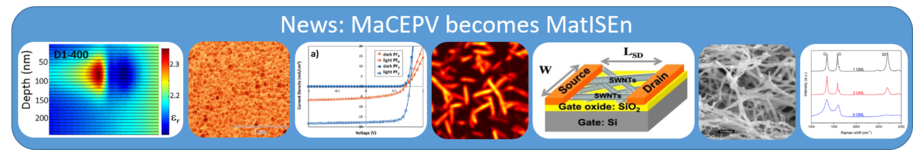
[[File:Bandeau news MaCEPV becomes MatISEn.png|x150px|link=https://matisen.icube.unistra.fr/en/index.php/News |News]] |
||
|} |
|} |
||
| Ligne 8 : | Ligne 8 : | ||
{|style="color: #4392D8;" width="100%" |
{|style="color: #4392D8;" width="100%" |
||
| style="width: 10%; | |
| style="width: 10%; | |
||
''<big>'''<big>Research activities of |
''<big>'''<big>Research activities of MatISEn team</big>'''</big>'' |
||
|} |
|} |
||
The activities of the ''' |
The activities of the '''MatISEn team''' are at the interface between the '''physics of electronic materials''' and the '''development of elementary semiconductor devices'''. They are based on the team's multidisciplinary skills in the '''development of thin films''' by physical or chemical methods, and in the '''fabrication and advanced characterization of electronic, photovoltaic or optical devices'''. <br> |
||
Our work aims to better understand the physical mechanisms governing the growth of nano-structured thin films, to modify materials by chemical or physical treatments and to study opto-electronic properties that have a strong impact on device operation (electrical conductivity, charge carrier mobility, band structure, absorption and emission spectra, etc.). The materials are generally designed to be integrated as an active element in elementary devices in order to improve their "performance" or to provide new functionalities. |
Our work aims to better understand the physical mechanisms governing the growth of nano-structured thin films, to modify materials by chemical or physical treatments and to study opto-electronic properties that have a strong impact on device operation (electrical conductivity, charge carrier mobility, band structure, absorption and emission spectra, etc.). The materials are generally designed to be integrated as an active element in elementary devices in order to improve their "performance" or to provide new functionalities. |
||
| Ligne 17 : | Ligne 17 : | ||
The materials studied (since the creation of the team) are, among others, crystalline or microcrystalline silicon, metal oxides based on zinc or tin, nitrides, oxides and oxynitrides, ferroelectric inorganic perovskites, carbon materials such as graphene or Diamond Like Carbon (DLC), semiconducting polymers and molecular semiconductors. It should be noted that organic materials are developed in close collaboration with several teams of chemists and physico-chemists from local public laboratories. |
The materials studied (since the creation of the team) are, among others, crystalline or microcrystalline silicon, metal oxides based on zinc or tin, nitrides, oxides and oxynitrides, ferroelectric inorganic perovskites, carbon materials such as graphene or Diamond Like Carbon (DLC), semiconducting polymers and molecular semiconductors. It should be noted that organic materials are developed in close collaboration with several teams of chemists and physico-chemists from local public laboratories which gave birth to the "Strasbourg electronic organic " consortium [http://stelorg.unistra.fr/ STELORG]. |
||
{|border="0" |
{|border="0" |
||
| |
| |
||
[[File: |
[[File:Imagetheme3.png|thumb|upright=0.7|gauche |link= Nanomaterials for electronics and sensors|[[Nanomaterials for electronics and sensors]]]] |
||
| |
| |
||
[[File:Imagetheme2.png|thumb|upright=0.9|gauche|link= |
[[File:Imagetheme2.png|thumb|upright=0.9|gauche|link= Materials and photovoltaic components|[[Materials and photovoltaic components]]]] |
||
| |
|||
[[File:Imagetheme3.png|thumb|upright=0.7|gauche |link= Functional materials and sensors|[[Functional materials and sensors]]]] |
|||
|} |
|} |
||
{| |
{| |
||
<big> The team's work is organised into |
<big> The team's work is organised into 2 main activities which are described in more detail below: </big> |
||
|} |
|} |
||
| Ligne 38 : | Ligne 35 : | ||
| style="width: 10%; | |
| style="width: 10%; | |
||
<big> |
<big> |
||
*''1. [[ |
*''1. [[Nanomaterials for electronics and sensors]]''<br> |
||
*''2. [[ |
*''2. [[Materials and photovoltaic components]]''<br> |
||
*''3. [[Functional materials and sensors]]''<br> |
|||
</big> |
</big> |
||
|} |
|} |
||
| Ligne 48 : | Ligne 44 : | ||
'''ICube UMR 7357 - Engineering science, computer science and imaging laboratory '''<br> |
'''ICube UMR 7357 - Engineering science, computer science and imaging laboratory '''<br> |
||
'''D-ESSP department - |
'''D-ESSP department - MatISEn team ''' <br> |
||
23, rue du Loess - BP 20 CR - 67037 STRASBOURG Cedex 2 - France <br> |
23, rue du Loess - BP 20 CR - 67037 STRASBOURG Cedex 2 - France <br> |
||
Tel.: +33 (0)3 88 10 6328 |
Tel.: +33 (0)3 88 10 6328 |
||
Dernière version du 19 mars 2024 à 14:31
|
Research activities of MatISEn team |
The activities of the MatISEn team are at the interface between the physics of electronic materials and the development of elementary semiconductor devices. They are based on the team's multidisciplinary skills in the development of thin films by physical or chemical methods, and in the fabrication and advanced characterization of electronic, photovoltaic or optical devices.
Our work aims to better understand the physical mechanisms governing the growth of nano-structured thin films, to modify materials by chemical or physical treatments and to study opto-electronic properties that have a strong impact on device operation (electrical conductivity, charge carrier mobility, band structure, absorption and emission spectra, etc.). The materials are generally designed to be integrated as an active element in elementary devices in order to improve their "performance" or to provide new functionalities.
The materials studied (since the creation of the team) are, among others, crystalline or microcrystalline silicon, metal oxides based on zinc or tin, nitrides, oxides and oxynitrides, ferroelectric inorganic perovskites, carbon materials such as graphene or Diamond Like Carbon (DLC), semiconducting polymers and molecular semiconductors. It should be noted that organic materials are developed in close collaboration with several teams of chemists and physico-chemists from local public laboratories which gave birth to the "Strasbourg electronic organic " consortium STELORG.
|
|
ICube UMR 7357 - Engineering science, computer science and imaging laboratory
D-ESSP department - MatISEn team
23, rue du Loess - BP 20 CR - 67037 STRASBOURG Cedex 2 - France
Tel.: +33 (0)3 88 10 6328
© 2013 ICube - Website created by ICube - Legal notice