« Gallery Thomas Fix » : différence entre les versions
Aller à la navigation
Aller à la recherche
Aucun résumé des modifications |
Aucun résumé des modifications |
||
| Ligne 1 : | Ligne 1 : | ||
<gallery mode="packed" widths=400px heights=400px> |
<gallery mode="packed" widths=400px heights=400px> |
||
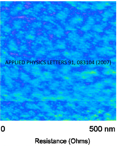
Image:tf01.png|''Local resistance through a tunnel barrier (Lévy flights, CTAFM)'' |
Image:tf01.png|''Local resistance through a tunnel barrier (Lévy flights, CTAFM)'' |
||
Image:tf02.png|'' |
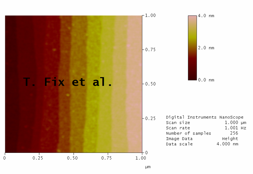
Image:tf02.png|''Atomic steps of an oxide substrate (AFM)'' |
||
Image:tf03.jpg|'' |
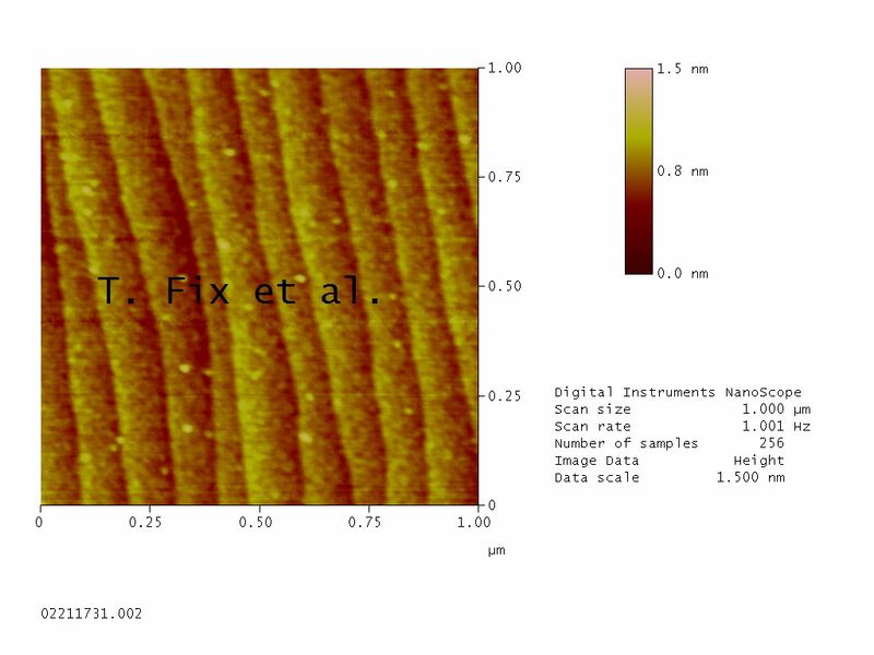
Image:tf03.jpg|''Atomic steps of an oxide substrate (AFM)'' |
||
Image:tf04.jpg|'' |
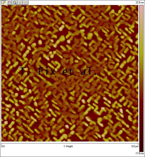
Image:tf04.jpg|''Thin film oxide (AFM)'' |
||
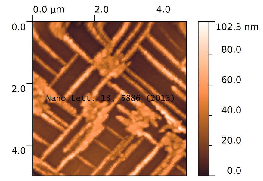
Image:tf05.jpg|'' |
Image:tf05.jpg|''Oxide nanocomposite (AFM)'' |
||
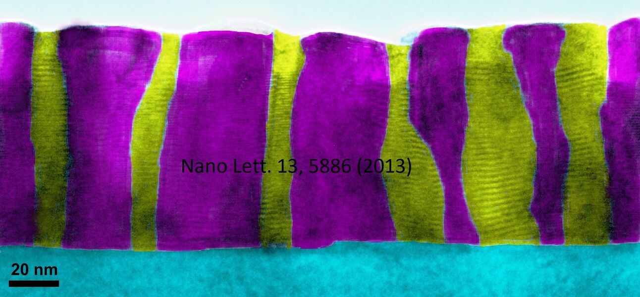
Image:tf19b.jpg|'' |
Image:tf19b.jpg|''Self-assembled epitaxial vertically aligned structures of La2CoMnO6-ZnO (TEM)'' |
||
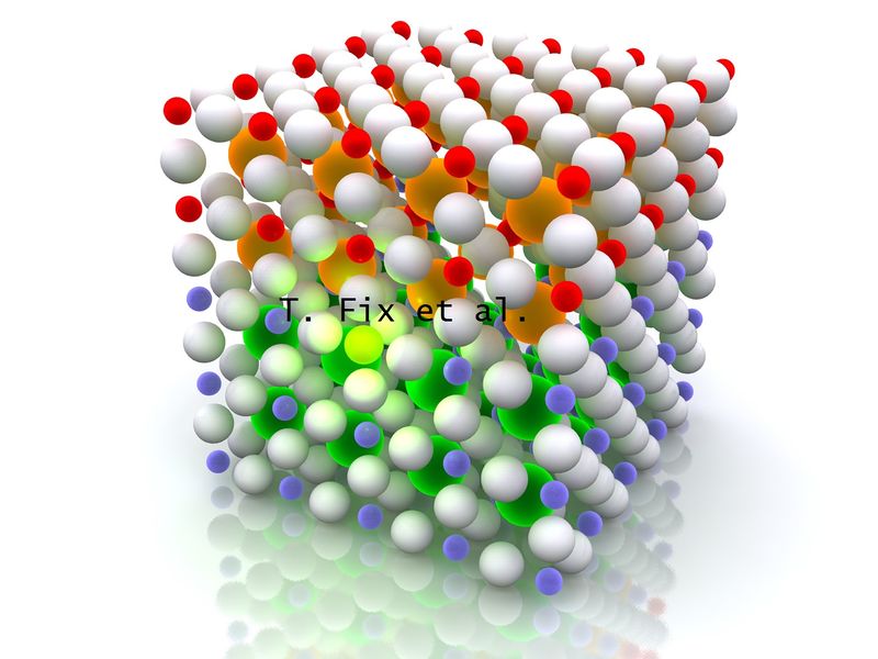
Image:tf06.jpg|'' |
Image:tf06.jpg|''Two-dimensional electron gas at the interface'' |
||
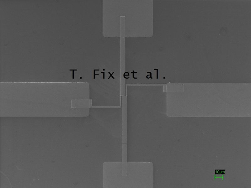
Image:tf07.jpg|'' |
Image:tf07.jpg|''Electron lithography for spin-FET'' |
||
Image:tf08.jpg|'' |
Image:tf08.jpg|''Electron lithography for spin-FET'' |
||
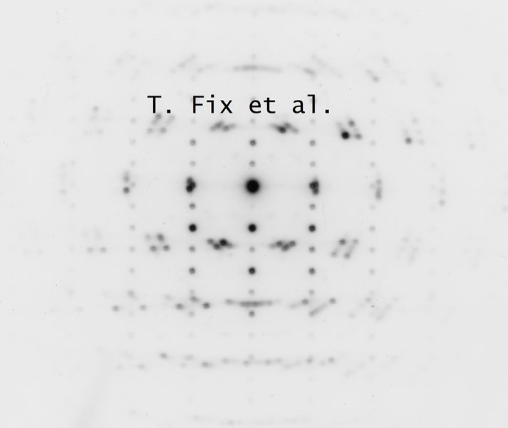
Image:tf09.jpg|'' |
Image:tf09.jpg|''Selected area diffraction of SnTiO3 film (TEM)'' |
||
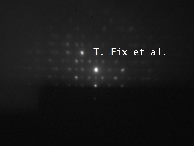
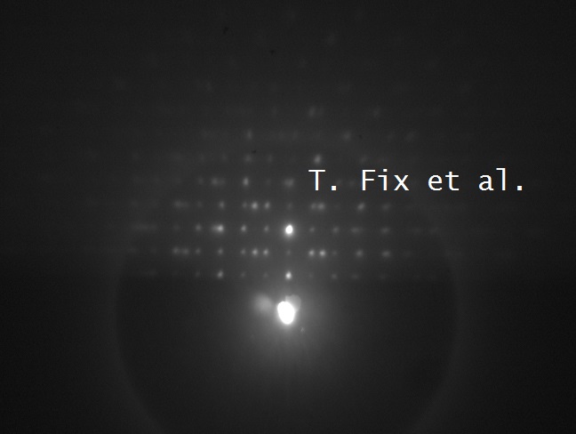
Image:tf10.jpg|'' |
Image:tf10.jpg|''RHEED image of an epitaxial thin film'' |
||
Image:tf11.jpg|'' |
Image:tf11.jpg|''RHEED image of an epitaxial thin film'' |
||
Image:tf12.jpg|'' |
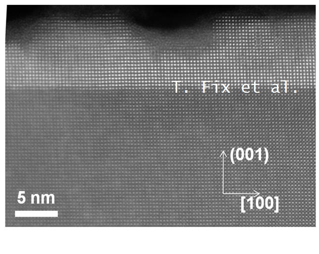
Image:tf12.jpg|''Cross-section of a LaAlO3/SrTiO3 interface (HRTEM)'' |
||
Image:tf13.jpg|'' |
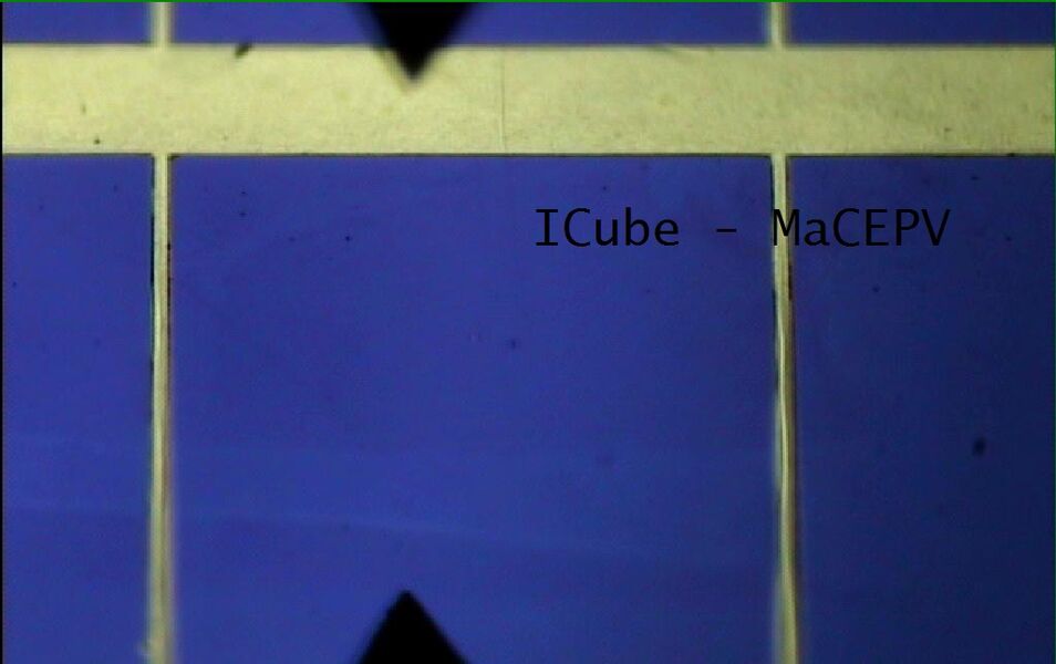
Image:tf13.jpg|''c-Si solar cell made in MaCEPV'' |
||
Image:tf14.jpg|'' |
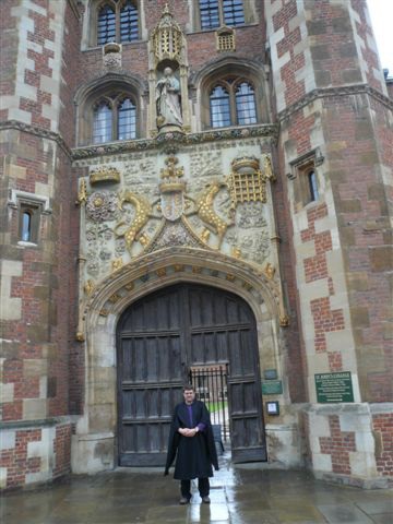
Image:tf14.jpg|''St John's college, Cambridge'' |
||
Image:tf15.jpg|'' |
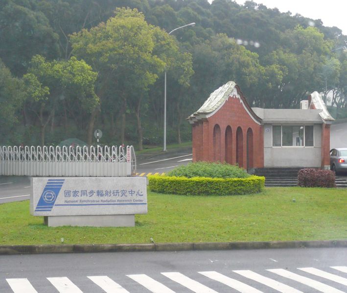
Image:tf15.jpg|''Taiwan Synchrotron'' |
||
Image:tf16.jpg|'' |
Image:tf16.jpg|''US boats with PV and wind'' |
||
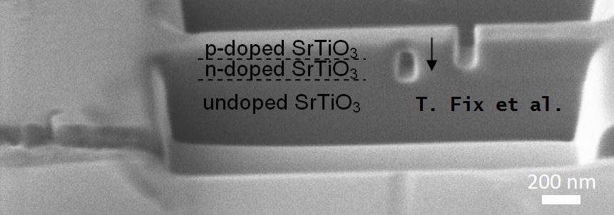
Image:tf17b.jpg|'' |
Image:tf17b.jpg|''Nanopatterned diode (FIB)'' |
||
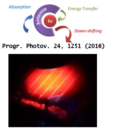
Image:tf18.jpg|'' |
Image:tf18.jpg|''Encapsulant functionalised with photon conversion'' |
||
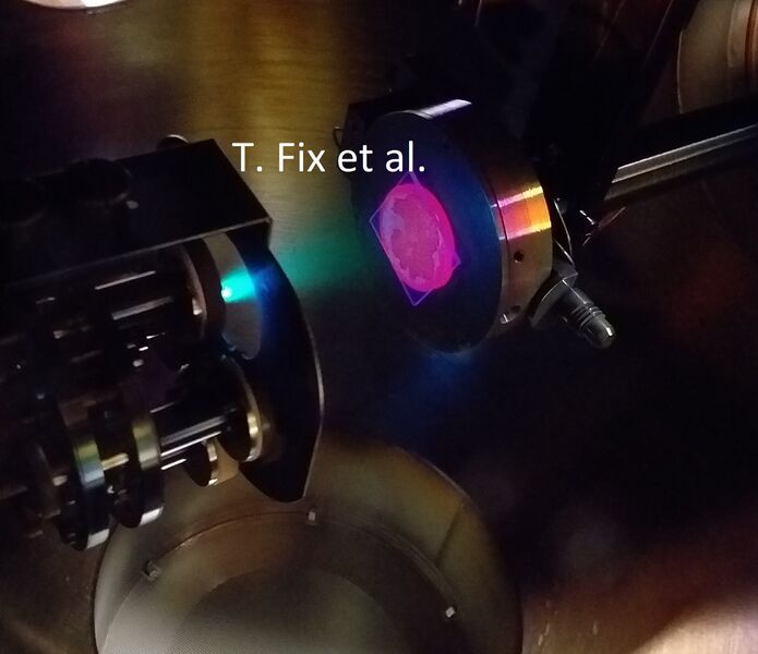
Image:Tf20b.jpg|'' |
Image:Tf20b.jpg|''Plasma during pulsed laser deposition (PLD)'' |
||
</gallery> |
</gallery> |
||


