« Gallery Thomas Fix » : différence entre les versions
Aucun résumé des modifications |
Aucun résumé des modifications |
||
| (32 versions intermédiaires par le même utilisateur non affichées) | |||
| Ligne 1 : | Ligne 1 : | ||
<gallery mode="packed" widths=400px heights=400px> |
|||
<slideshow sequence="random" transition="fade" refresh="10000"> |
|||
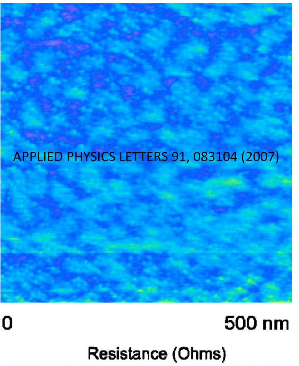
Image:tf01.png|''Local resistance through a tunnel barrier (Lévy flights, CTAFM)'' |
|||
<div>[[Image:tf01.png|thumb|right|128px|Caption 1]]</div> |
|||
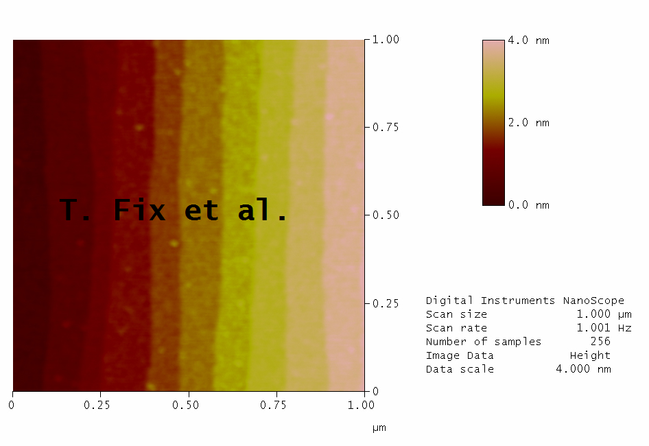
Image:tf02.png|''Atomic steps of an oxide substrate (AFM)'' |
|||
Image:tf03.jpg|''Atomic steps of an oxide substrate (AFM)'' |
|||
Image:tf04.jpg|''Thin film oxide (AFM)'' |
|||
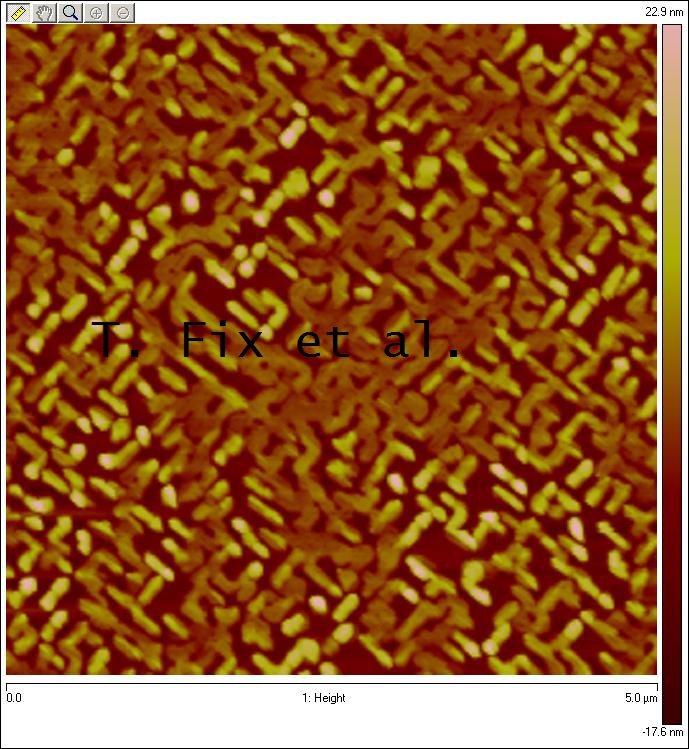
Image:tf05.jpg|''Oxide nanocomposite (AFM)'' |
|||
Image:tf19b.jpg|''Self-assembled epitaxial vertically aligned structures of La2CoMnO6-ZnO (TEM)'' |
|||
<div>[[Image:tf06.jpg|thumb|right|128px|Caption 3]]</div> |
|||
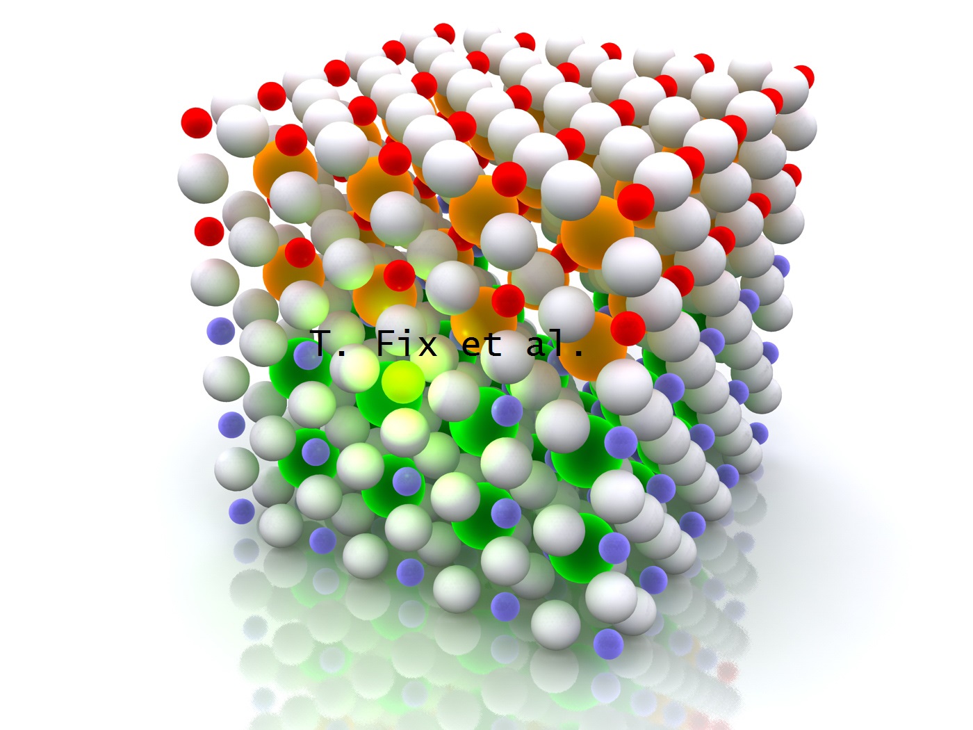
Image:tf06.jpg|''Two-dimensional electron gas at the interface'' |
|||
<div>[[Image:tf07.jpg|thumb|right|128px|Caption 3]]</div> |
|||
Image:tf07.jpg|''Electron lithography for spin-FET'' |
|||
Image:tf08.jpg|''Electron lithography for spin-FET'' |
|||
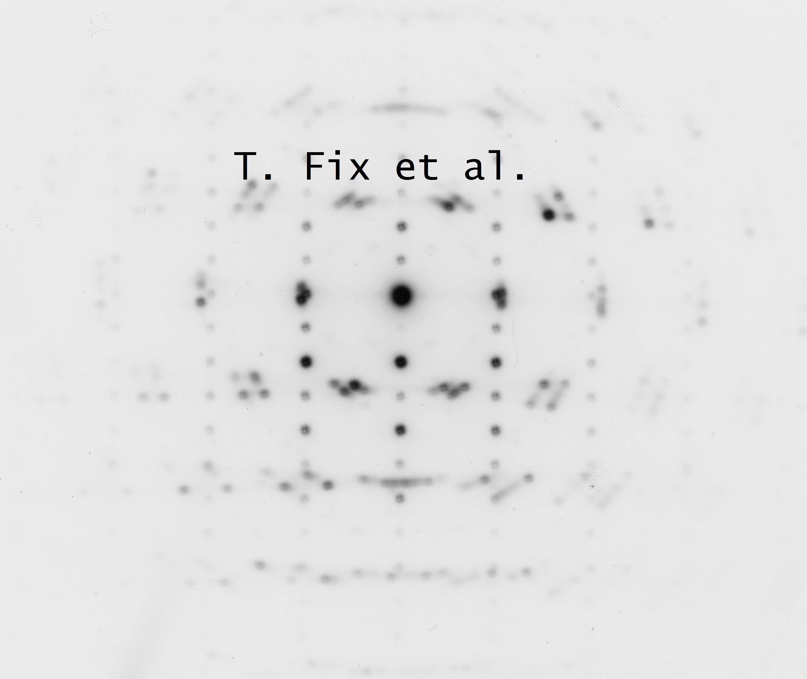
Image:tf09.jpg|''Selected area diffraction of SnTiO3 film (TEM)'' |
|||
<div>[[Image:tf10.jpg|thumb|right|128px|Caption 3]]</div> |
|||
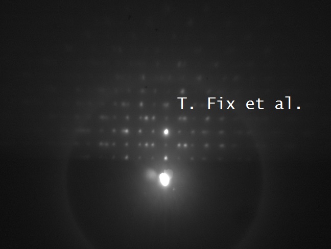
Image:tf10.jpg|''RHEED image of an epitaxial thin film'' |
|||
<div>[[Image:tf11.jpg|thumb|right|128px|Caption 3]]</div> |
|||
Image:tf11.jpg|''RHEED image of an epitaxial thin film'' |
|||
<div>[[Image:tf12.jpg|thumb|right|128px|Caption 3]]</div> |
|||
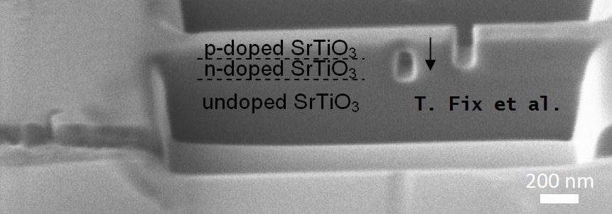
Image:tf12.jpg|''Cross-section of a LaAlO3/SrTiO3 interface (HRTEM)'' |
|||
<div>[[Image:tf13.jpg|thumb|right|128px|Caption 3]]</div> |
|||
Image:tf13.jpg|''c-Si solar cell made in MaCEPV'' |
|||
Image:tf14.jpg|''St John's college, Cambridge'' |
|||
</slideshow> |
|||
Image:tf15.jpg|''Taiwan Synchrotron'' |
|||
Image:tf16.jpg|''US boats with PV and wind'' |
|||
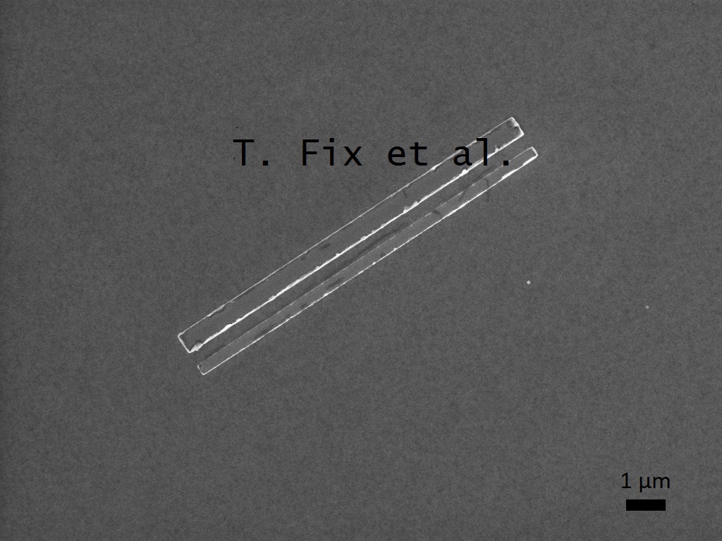
Image:tf17b.jpg|''Nanopatterned diode (FIB)'' |
|||
Image:tf18.jpg|''Encapsulant functionalised with photon conversion'' |
|||
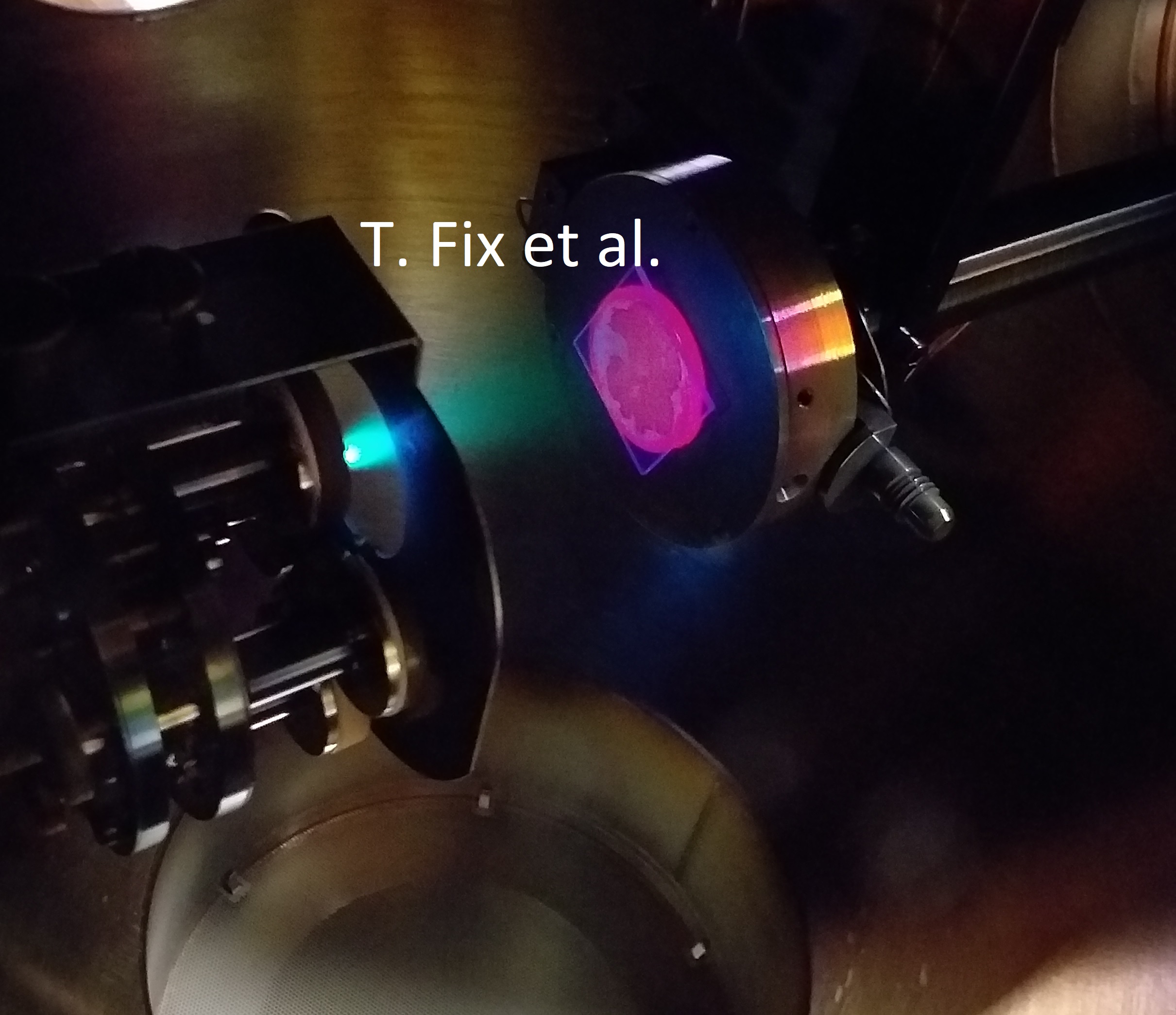
Image:Tf20b.jpg|''Plasma during pulsed laser deposition (PLD)'' |
|||
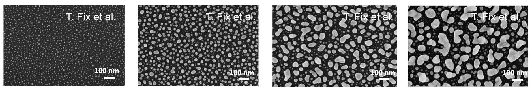
Image:AgNps.jpg|''Ag nanoparticles implanted in SiON'' |
|||
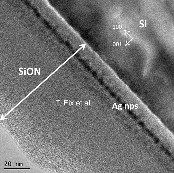
Image:Tf21.jpg|''Ag nanoparticles on SiON'' |
|||
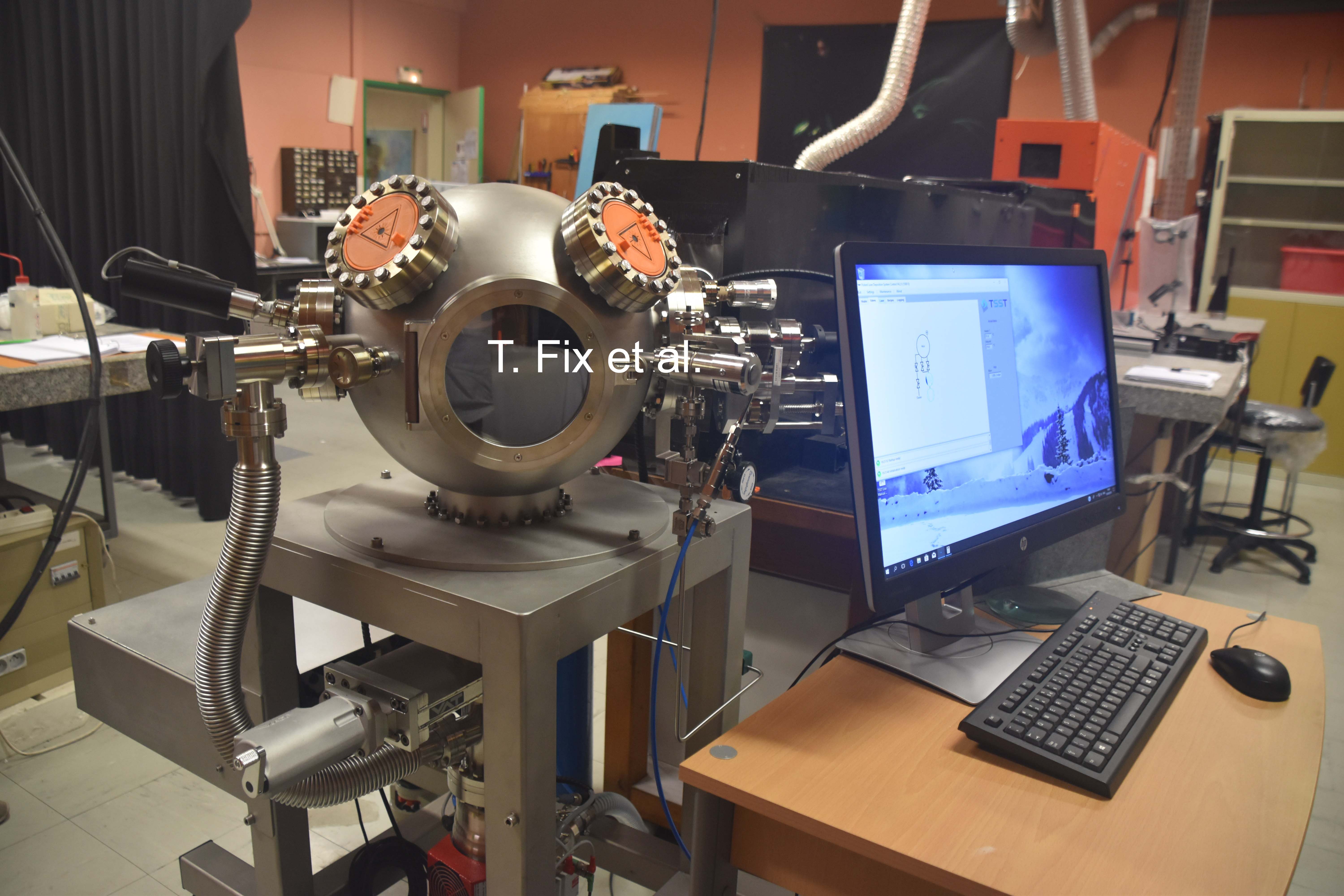
Image:Tf22.jpg|''Pulsed laser deposition (PLD) system'' |
|||
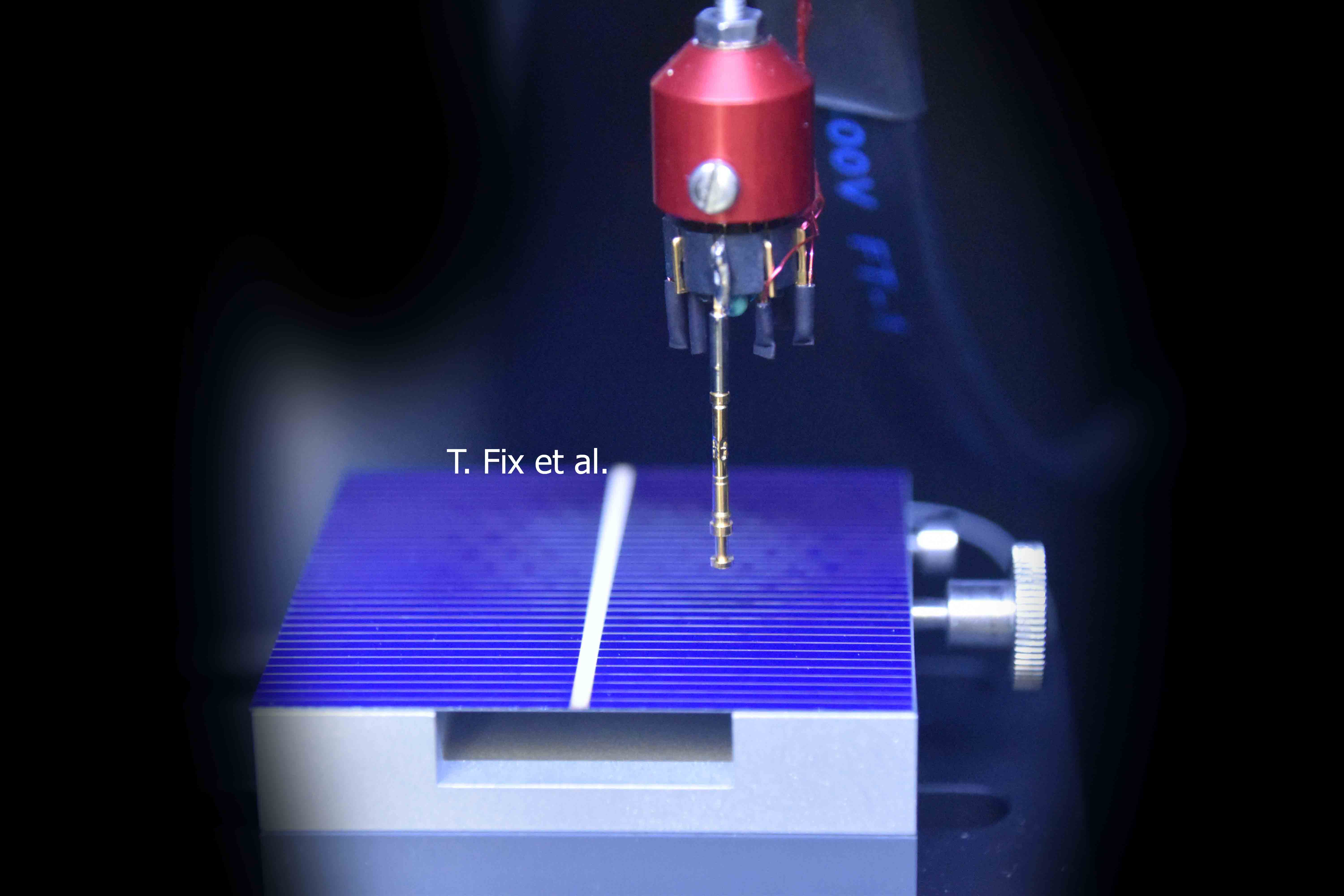
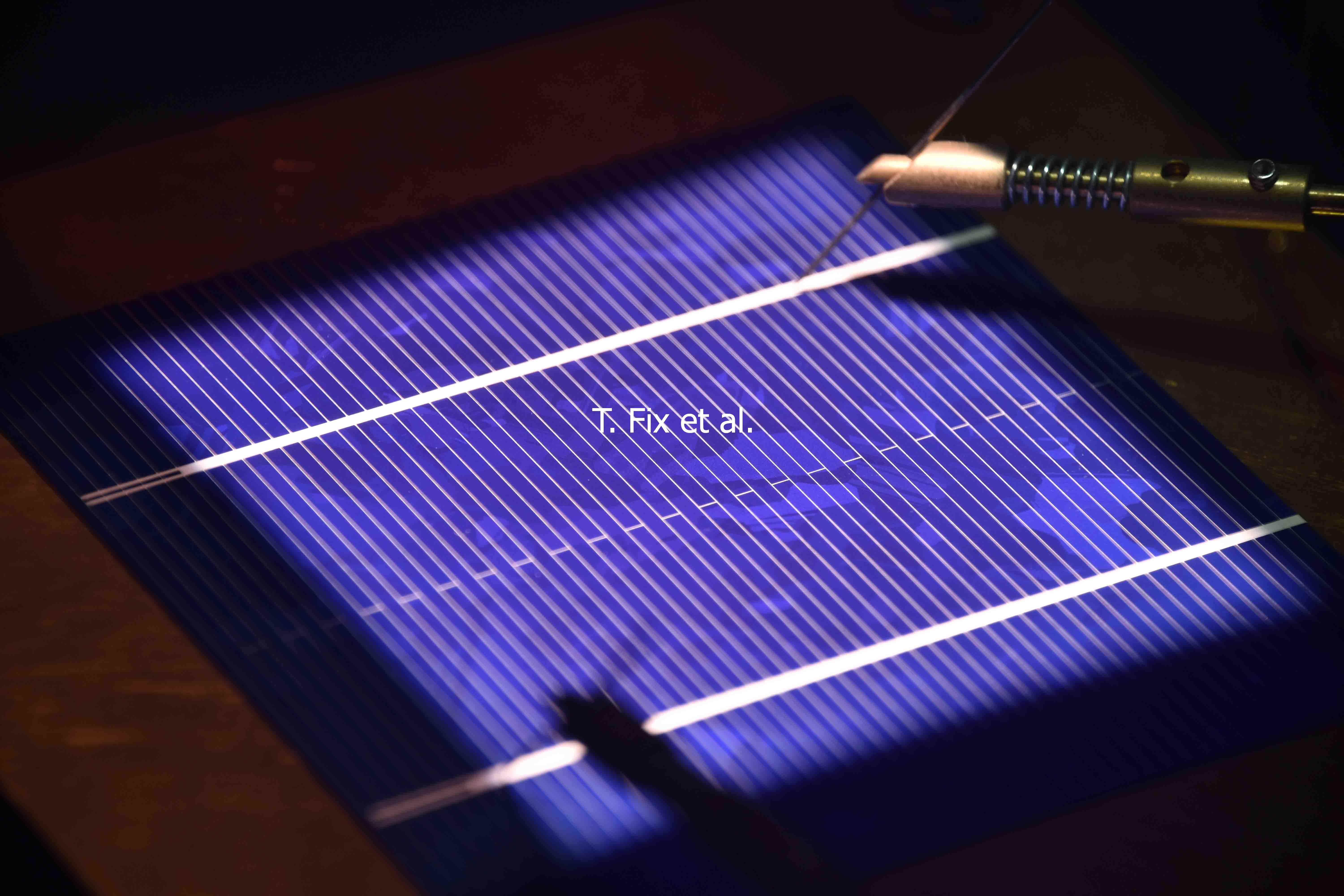
Image:Tf23.jpg|''Si solar cell in scanning Kelvin Probe'' |
|||
Image:Tf24.jpg|''Si solar cell in solar simulator'' |
|||
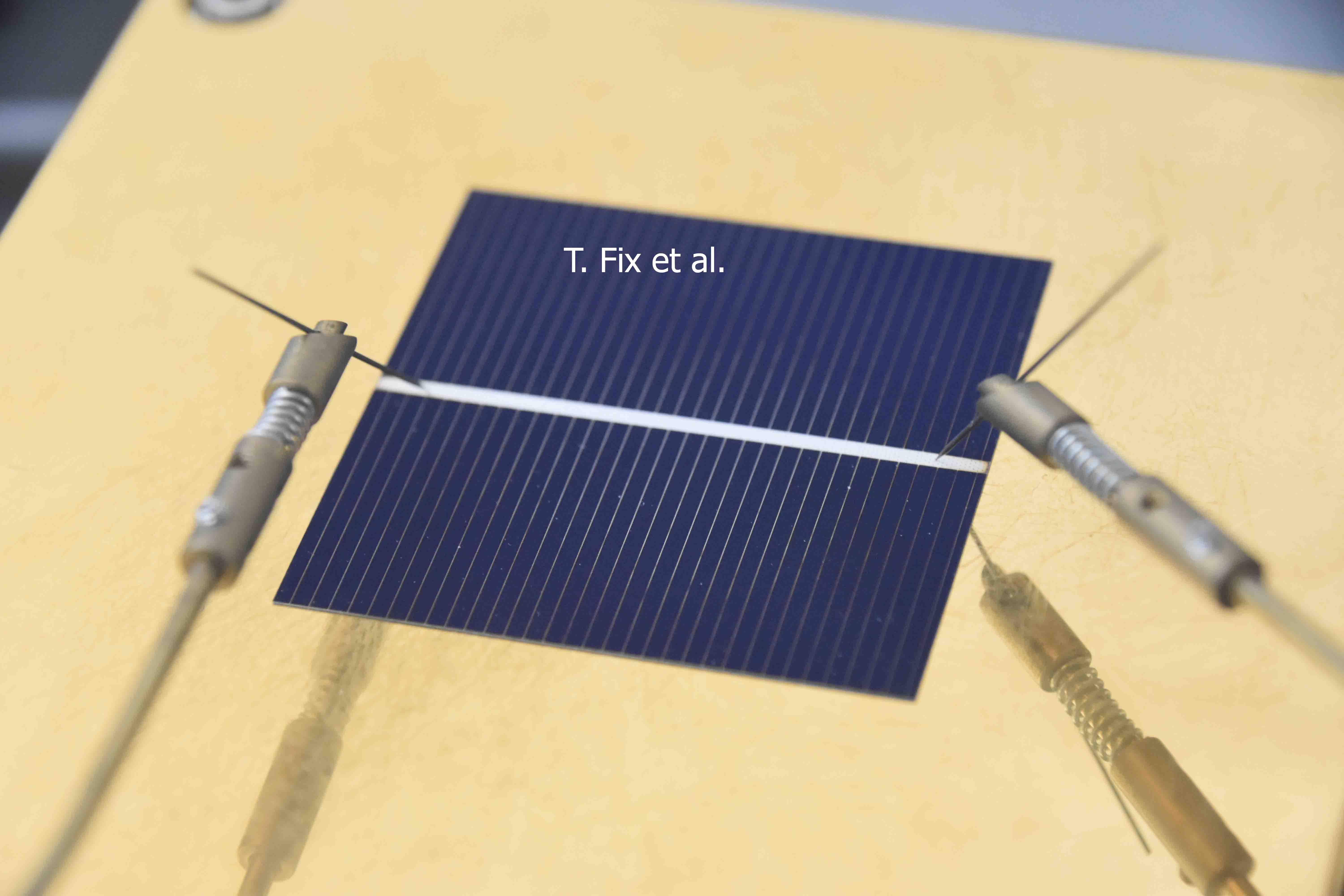
Image:Tf25.jpg|''Si solar cell for IV measurement'' |
|||
Image:Tf26.jpg|''Oxidized Cu2O solar cell'' |
|||
</gallery> |
|||
Dernière version du 21 avril 2023 à 05:13

Local resistance through a tunnel barrier (Lévy flights, CTAFM)
Atomic steps of an oxide substrate (AFM)
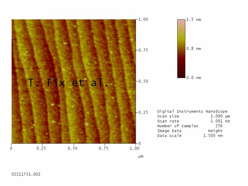
Atomic steps of an oxide substrate (AFM)
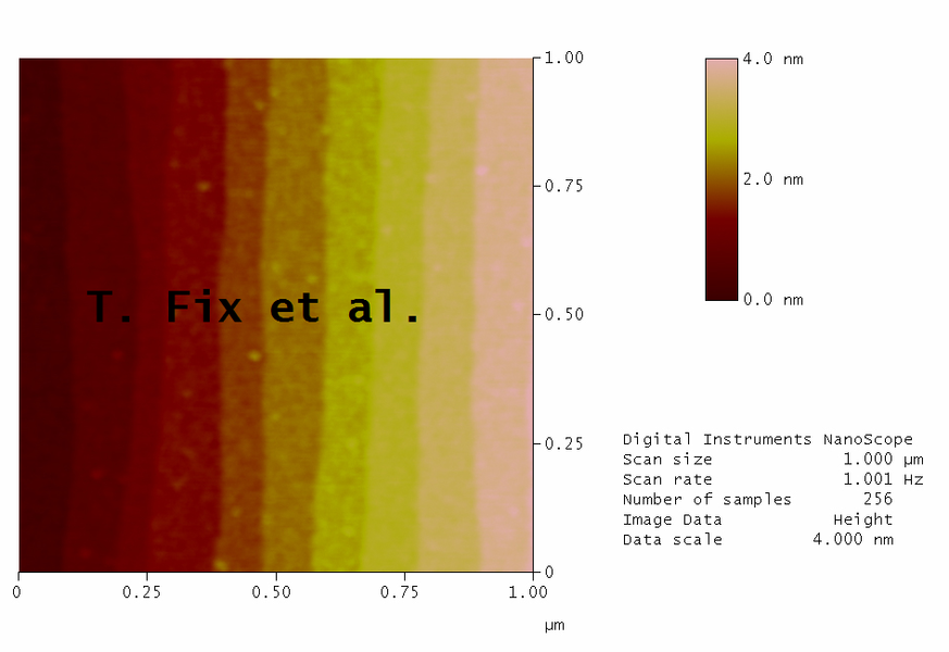
Thin film oxide (AFM)
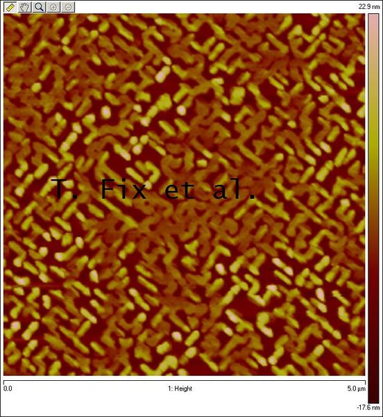
Oxide nanocomposite (AFM)
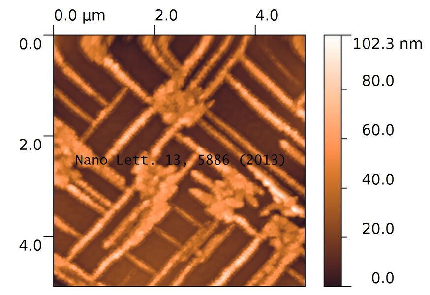
Self-assembled epitaxial vertically aligned structures of La2CoMnO6-ZnO (TEM)

Two-dimensional electron gas at the interface
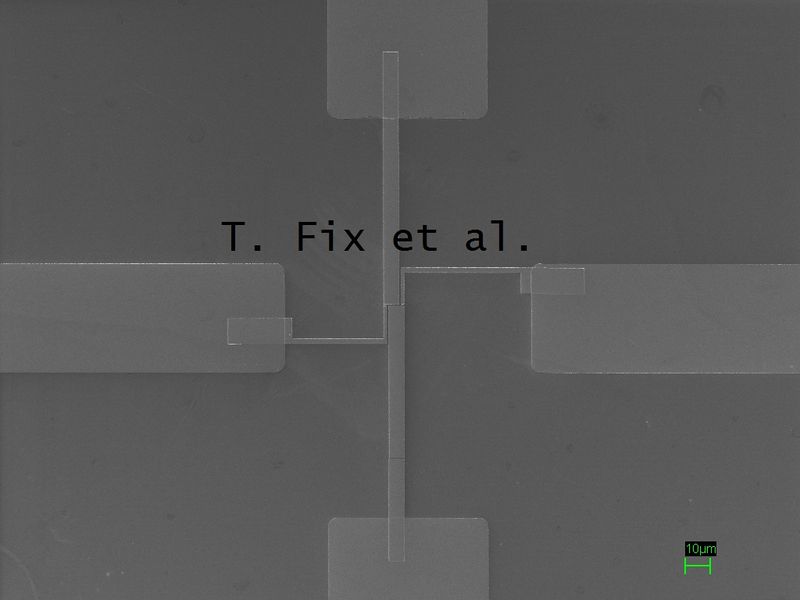
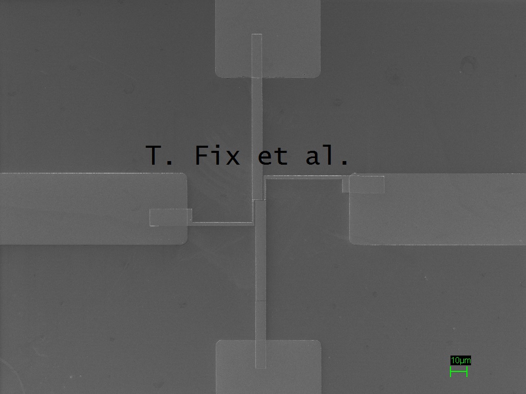
Electron lithography for spin-FET
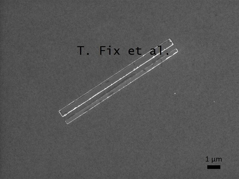
Electron lithography for spin-FET
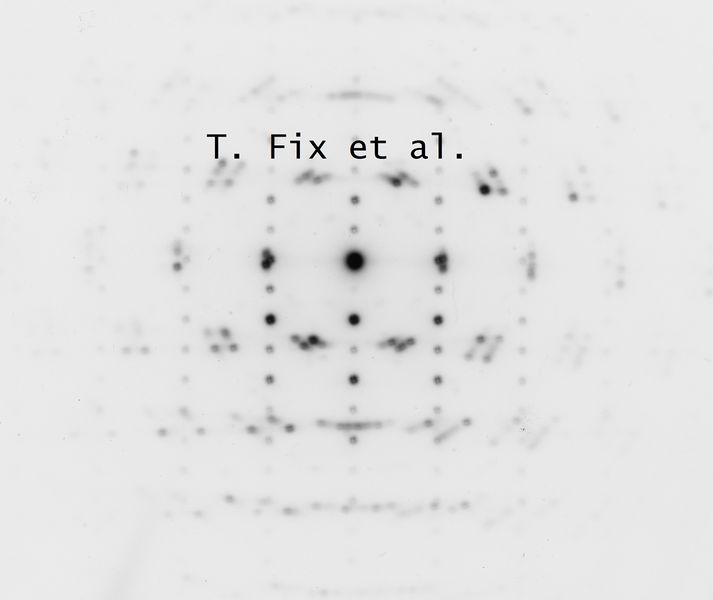
Selected area diffraction of SnTiO3 film (TEM)
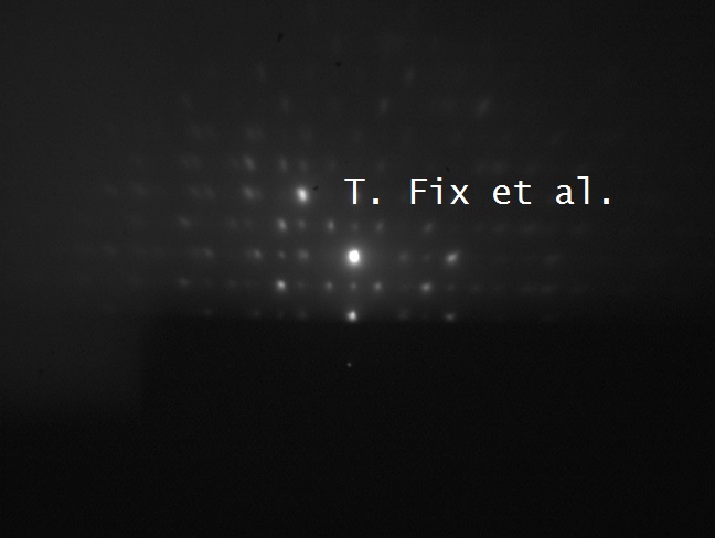
RHEED image of an epitaxial thin film

RHEED image of an epitaxial thin film
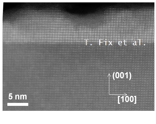
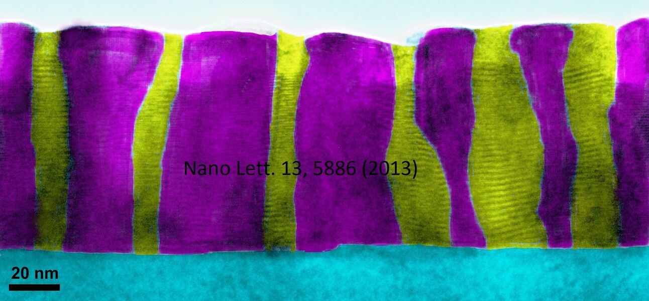
Cross-section of a LaAlO3/SrTiO3 interface (HRTEM)
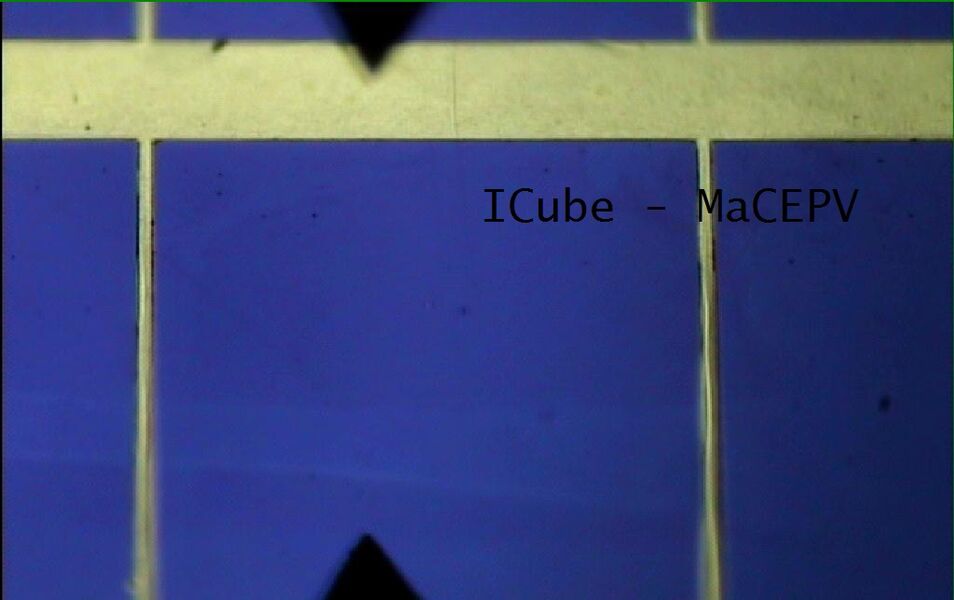
c-Si solar cell made in MaCEPV

St John's college, Cambridge
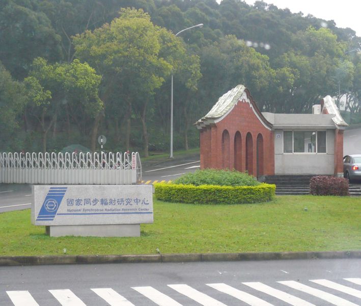
Taiwan Synchrotron

US boats with PV and wind
Nanopatterned diode (FIB)
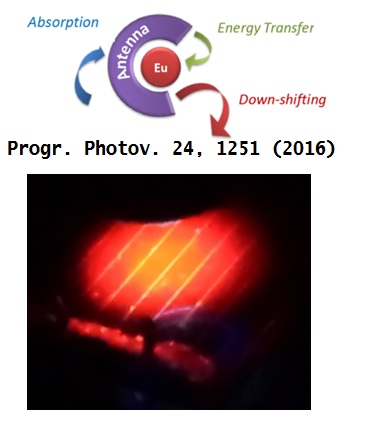
Encapsulant functionalised with photon conversion

Plasma during pulsed laser deposition (PLD)
Ag nanoparticles implanted in SiON

Ag nanoparticles on SiON

Pulsed laser deposition (PLD) system

Si solar cell in scanning Kelvin Probe

Si solar cell in solar simulator
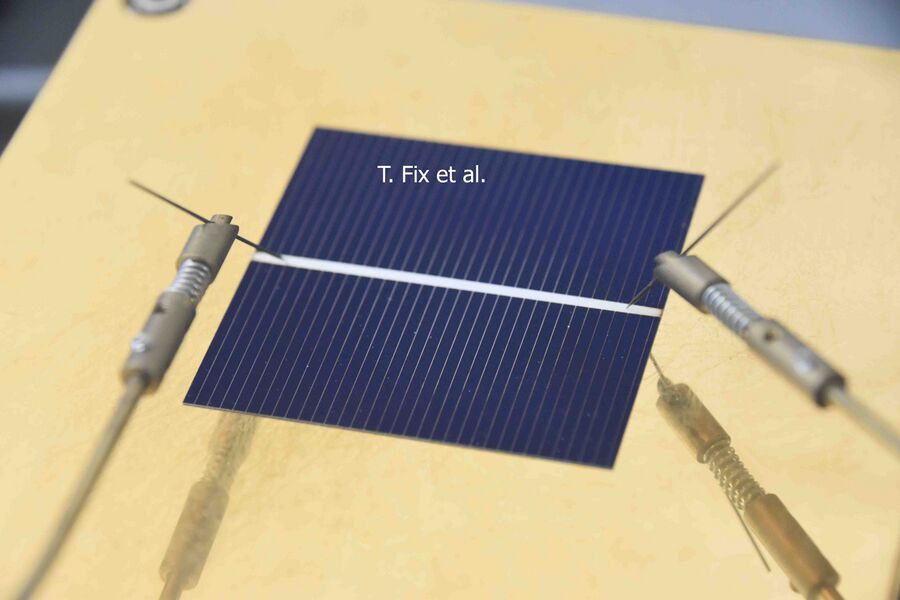
Si solar cell for IV measurement
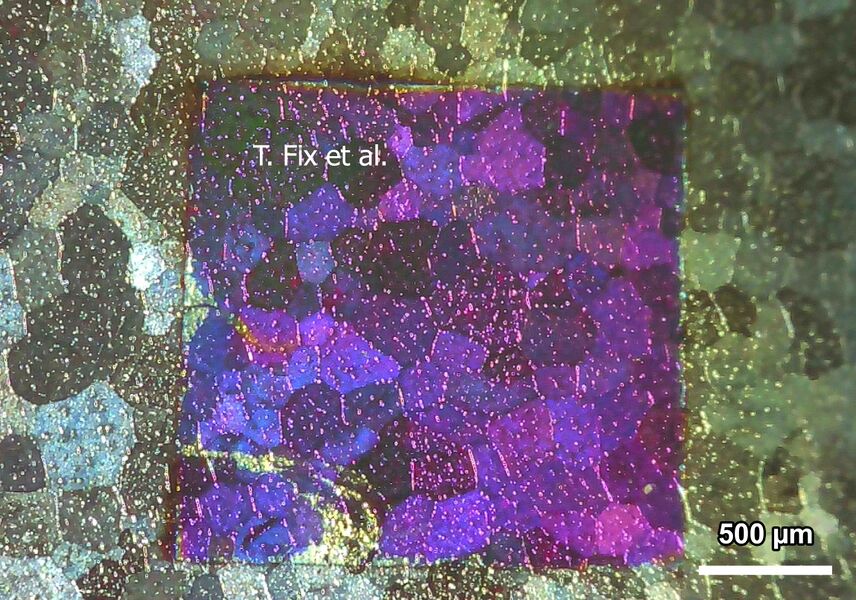
Oxidized Cu2O solar cell