« Photovoltaic materials and devices » : différence entre les versions
Aucun résumé des modifications |
Aucun résumé des modifications |
||
| Ligne 1 : | Ligne 1 : | ||
[[fr:Matériaux et composants photovoltaïques]] |
[[fr:Matériaux et composants photovoltaïques]] |
||
<span id="bidule"> </span> |
|||
<table border="0" width="100%"> |
|||
<tr valign=top><td width="25%">[[File:Cellule6aRed2.jpg]]</td> |
|||
<td><p><em><strong>T. Heiser</strong>, P. Lévêque, E. Steveler, N. Zimmermann, S. Fall</em></p></td></tr> |
|||
</table> |
|||
Although the part of photovoltaics in the production of renewable energy is still largely due to the traditional crystalline silicon sector, many so-called "emerging" technologies are the subject of research work around the world and aim to '''reduce the cost of photovoltaics''' and '''widen its field of application'''. In this context, the development of new thin-film materials with outstanding optical, electronic and mechanical properties plays a key role. Our team participates in these efforts by developing '''new inorganic and organic materials''', studying their '''fundamental properties''', and implementing them in the '''manufacturing of innovative photovoltaic components'''. |
|||
<p>This theme is dedicated to the field of organic electronics, with the aim to develop novel organic semiconductor devices for photovoltaic and sensor applications. The activity is highly multidisciplinary and relies on strong collaborations with teams from neighboring laboratories ([http://icpees.unistra.fr ICPEES], [http://www-ics.u-strasbg.fr/?lang=en ICS], [http://www-ipcms.u-strasbg.fr/?lang=en IPCMS], [http://www.is2m.uha.fr/index.php?it1=acc&langue=en IS2M]). The group also established privileged relationships with other neighbouring teams through the network [http://www.mateohpv.fr MATEOH-PV] ("MAtériaux et TEchnologies Organiques et Hybrides pour le PhotoVoltaïque") in which our group plays a major role.</p> |
|||
<p>It is our main purpose to investigate the optoelectronic properties of novel organic materials, that have been designed and synthesised by chemists to fulfill a specific function (i.e. charge transport, light absorption, chemical recognition...), and to implement them as active material into dedicated devices. In order to carry out these studies, the laboratory recently acquired a technological platform to elaborate and characterise organic components under a controlled atmosphere. This platform is made up of several glove boxes that are coupled and equipped both with organic and inorganic thin film deposition tools (by wet process or vacuum evaporation) and characterisation instruments.</p> |
|||
<p>Three research topics are currently being considered: donor-acceptor bulk heterojunction solar cells for renewable electricity production, charge transport in organic semiconductors, and organic field effect transistors for chemical sensors.</p> |
|||
__TOC__ |
|||
=Developed topics= |
|||
<br> |
|||
== Towards the industrialization of organic photovoltaics == |
|||
{|style="color: #4392D8;" width="100%" |
|||
| style="width: 10%; | |
|||
''' Persons involved: P. Lêvèque, T. Heiser, J. Wang, S. Fall''' <br> |
|||
'''Collaborations: N. Leclerc (ICPEES), B. Heinrich (IPCMS), S. Méry (IPCMS), M. Kohlstädt (FMF, Université de Freiburg), U. Würfel (Fraunhofer ISE).''' |
|||
|} |
|||
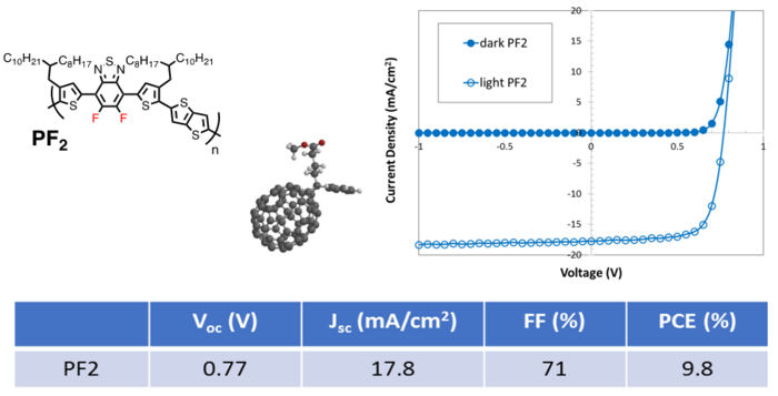
An electron-donor polymer designed and synthesized at the Cronenbourg campus (PF2) gives high conversion efficiencies (about 10%) when mixed with the PC71BM electron acceptor. This project aims to demonstrate its industrial potential by developing several approaches: <br> |
|||
- Polymer production at the gram scale or more, <br> |
|||
- Avoid halogenated solvents for the wet deposition of the active layer,<br> |
|||
- Avoid rare materials (e.g. Indium) when making transparent conductive electrodes,<br> |
|||
- Go from laboratory scale (12 mm2) to large areas (> 60 cm2). |
|||
[[File:Image6.png|center|700px]] |
|||
<div class="center"> Figure 1: Structure of PF2 and PC71BM (top left), characteristics (J-V) under darkness and standard illumination (AM1.5G (100mW/cm2)) (top right) and corresponding photovoltaic parameters (bottom). |
|||
</div> |
|||
[[#bidule|Back to contents]] |
|||
== Ternary mixtures for improved yield and/or stability == |
|||
{|style="color: #4392D8;" width="100%" |
|||
| style="width: 10%; | |
|||
''' Persons involved: P. Lêvèque, T. Heiser, A. Labiod, S. Fall''' <br> |
|||
'''Collaborations: N. Leclerc (ICPEES), B. Heinrich (IPCMS), S. Méry (IPCMS), F. Zhang (University Jiaotong of Beijing).''' |
|||
|} |
|||
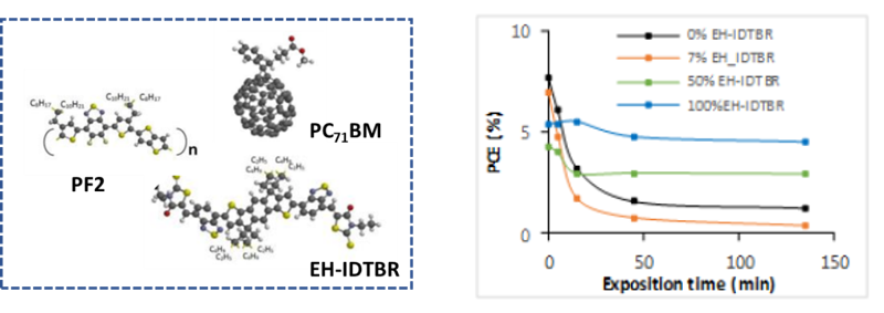
Study ternary mixtures in the active layer to increase the photovoltaic conversion efficiency and/or device stability. Starting from PF2, conversion efficiencies greater than 12% were obtained using two electron-donor polymers (PF2 and J71) and a non-fullerene derived electron acceptor (Y6) of complementary absorption spectra. Using one electron donor polymer (PF2) and two acceptors (PC71BM and EH-IDTBR), good light stability was observed. Better understanding of the influence of ternary mixtures in terms of solid state structure and boundary electron level tuning is a lock that needs to be lifted to jointly achieve high yields and sufficient stability. |
|||
[[File:Image7.png|center]] |
|||
<div class="center"> Figure 2: Structure of PF2, J71 and Y6 (left), complementarity of absorption spectra (middle) and boundary levels (right). |
|||
</div> |
|||
[[File:Image8.png|center]] |
|||
<div class="center"> Figure 3: Structure of PF2, PC71BM and EH-IDTBR (left), stability of conversion efficiency as a function of illumination time (right). |
|||
</div> |
|||
[[#bidule|Back to contents]] |
|||
== Dynamics of excitons and charge carriers == |
|||
{|style="color: #4392D8;" width="100%" |
|||
| style="width: 10%; | |
|||
''' Persons involved: E. Steveler, T. Heiser, J. Jing''' <br> |
|||
'''Collaborations: N. Leclerc (ICPEES), B. Heinrich (IPCMS), S. Méry (IPCMS), W. Uhring (ICube, SMH), Pascal Didier (LBP).''' |
|||
|} |
|||
The efficiency of organic photovoltaic (OPV) devices is currently limited by the short lifetime (< 1 ns) and short diffusion length (a few nm) of the photogenerated excitons. The development of organic materials with long diffusion lengths (typically > 10 nm) is therefore proving to be a particularly interesting way to improve charge transport and should lead to an improvement in OPV performance. In thin films, the dynamics of excitons and charge carriers, crucial for the operation of OPV devices, is controlled by intermolecular interactions and depend in a non-trivial way on the molecular organization in the solid state. <br> |
|||
In this context, we are studying families of organic molecules with different side chains and heat treatment conditions, allowing us to obtain molecular structures and various crystalline orders (liquid crystal, needles or crystalline grains...). We are thus studying the influence of molecular organization and self-assembly on the dynamics of excitons in order to improve the performance of OPV devices. |
|||
[[File:Image9.png|center]] |
|||
<div class="center"> Figure 4: Continuous-wave photoluminescence (PL) map for (left) amorphous and (middle) crystalline thin films. (right) Time-resolved PL spectra measured on amorphous and crystalline thin films. |
|||
</div> |
|||
[[#bidule|Back to contents]] |
|||
== Downshifting and downconversion for solar cells == |
|||
{|style="color: #4392D8;" width="100%" |
|||
| style="width: 10%; | |
|||
''' Persons involved: T. Fix, G. Ferblantier, A. Slaoui ''' <br> |
|||
'''Collaborations: IPVF, IPHC, IJL''' |
|||
|} |
|||
Increasing the conversion efficiency requires the complete use of the solar spectrum by the conversion layer. One of the possible solutions is impurity cells or intermediate band cells, in which a modification of the active part of the cell is necessary. Another original idea consists in the modification of the incident spectrum by energy conversion of its photons, either by downshifting (DS, one UV photon is converted into one visible or near-infrared photon), down-conversion (DC, one UV photon is converted into two visible or near-infrared photons) or upconversion (UC, two infrared photons are converted into one visible photon).<br> |
|||
We investigate several downshifting and downconversion systems, either in the form of bulk, oxide thin films, and polymers functionalized with coordination complexes. <br> |
|||
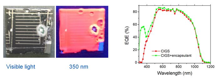
So far, an increase of 0.8 points in the efficiency of CIGS solar cells has been demonstrated by ICube, IPHC and IPVF thanks to the downshifting concept (example from 13.5 to 14.3 % conversion efficiency). |
|||
[[File:Figure5-fix.jpg|center|700px]] |
|||
<div class="center"> Figure 5: Impact of the Eu(tta)3(tppo)2 complex in an EVA polymer on CIGS solar cells. |
|||
</div> |
|||
[[#bidule|Back to contents]] |
|||
== Novel oxides for photovoltaic absorbers == |
|||
{|style="color: #4392D8;" width="100%" |
|||
| style="width: 10%; | |
|||
''' Persons involved: T. Fix, C. Venugopalan Kartha, G. Ferblantier, D. Muller, A. Slaoui ''' <br> |
|||
'''Collaborations: IPCMS, Purdue University, University of Bologna, Tokyo University of Science''' |
|||
|} |
|||
Inorganic photovoltaic thin film technologies are mainly based on CdTe, amorphous Si and CuInxGa1-xSe2 (CIGS). A major recent breakthrough was obtained with hybrid perovskite solar cells, with conversion efficiencies higher than 20% using a very small area but not stabilized. Another possible path is the use of metal oxides based on abundant elements, that are generally stable and non-toxic. |
|||
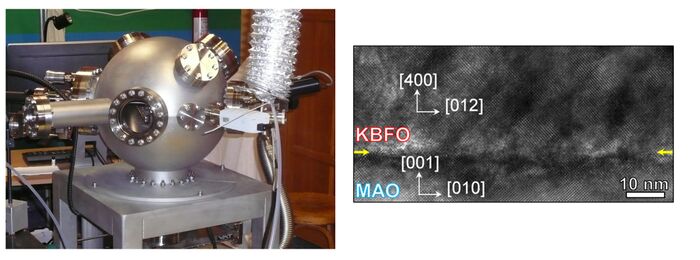
We use pulsed laser deposition (PLD) to investigate novel oxide absorbers for solar cells. <br> |
|||
The oxides investigated must have a rather low bandgap to match the solar spectrum. The oxides investigated are LaVO3, Cu2O, KBiFe2O5, h-TbMnO3 and Bi2FeCrO6. For the latter, ferroelectricity is established and plays an important role in the photovoltaic properties. Ferroelectric materials are under intense scrutiny for photovoltaic applications, following the demonstration of above 8% conversion efficiency in FE-based solar cells. In these cells, there is no need for a p-n junction because the electric polarization from ferroelectricity is responsible for the charge separation. |
|||
[[File:Figure6-fix.jpg|center|700px]] |
|||
<div class="center"> Figure 6: (left) Pulsed laser deposition system for oxides. (right) Transmission electron microscopy cross-sectional image showing epitaxy of KBiFe2O5 on MgAl2O4 (001). |
|||
</div> |
|||
[[#bidule|Back to contents]] |
|||
== Silicon clathrate films == |
|||
{|style="color: #4392D8;" width="100%" |
|||
| style="width: 10%; | |
|||
''' Persons involved: T. Fix, R. Vollondat, S. Roques, D. Muller, A. Slaoui ''' <br> |
|||
'''Collaborations: IPCMS, INL''' |
|||
|} |
|||
Common forms of elemental silicon (mono-, multi-crystalline and amorphous) play a foundational role in the field of electronics and the underlying technologies are well mastered. A promising alternative is based on an allotrope of silicon: silicon clathrates. They are similar to carbon fullerenes as they form hollow spheres. ICube is one of the few laboratories that can elaborate such material in the form of films. The electronic and optical properties of some of these clathrates are strongly different to the “standard” silicon as they can provide a direct bandgap, paving the way for novel applications in electronics and optoelectronics. Applications in sodium-ion batteries are also emerging. Not only the size of the clathrates but also the presence of doping atoms can dramatically modify their properties. Ion implantation available at ICube is used to modify the properties of the clathrates. |
|||
[[File:Figure7-fix.jpg|center|450px]] |
|||
<div class="center"> Figure 7: Silicon clathrate film on c-Si (001). |
|||
</div> |
|||
[[#bidule|Back to contents]] |
|||
Version du 12 mars 2020 à 10:51
Although the part of photovoltaics in the production of renewable energy is still largely due to the traditional crystalline silicon sector, many so-called "emerging" technologies are the subject of research work around the world and aim to reduce the cost of photovoltaics and widen its field of application. In this context, the development of new thin-film materials with outstanding optical, electronic and mechanical properties plays a key role. Our team participates in these efforts by developing new inorganic and organic materials, studying their fundamental properties, and implementing them in the manufacturing of innovative photovoltaic components.
Developed topics
Towards the industrialization of organic photovoltaics
|
Persons involved: P. Lêvèque, T. Heiser, J. Wang, S. Fall
|
An electron-donor polymer designed and synthesized at the Cronenbourg campus (PF2) gives high conversion efficiencies (about 10%) when mixed with the PC71BM electron acceptor. This project aims to demonstrate its industrial potential by developing several approaches:
- Polymer production at the gram scale or more,
- Avoid halogenated solvents for the wet deposition of the active layer,
- Avoid rare materials (e.g. Indium) when making transparent conductive electrodes,
- Go from laboratory scale (12 mm2) to large areas (> 60 cm2).
Ternary mixtures for improved yield and/or stability
|
Persons involved: P. Lêvèque, T. Heiser, A. Labiod, S. Fall
|
Study ternary mixtures in the active layer to increase the photovoltaic conversion efficiency and/or device stability. Starting from PF2, conversion efficiencies greater than 12% were obtained using two electron-donor polymers (PF2 and J71) and a non-fullerene derived electron acceptor (Y6) of complementary absorption spectra. Using one electron donor polymer (PF2) and two acceptors (PC71BM and EH-IDTBR), good light stability was observed. Better understanding of the influence of ternary mixtures in terms of solid state structure and boundary electron level tuning is a lock that needs to be lifted to jointly achieve high yields and sufficient stability.
Dynamics of excitons and charge carriers
|
Persons involved: E. Steveler, T. Heiser, J. Jing
|
The efficiency of organic photovoltaic (OPV) devices is currently limited by the short lifetime (< 1 ns) and short diffusion length (a few nm) of the photogenerated excitons. The development of organic materials with long diffusion lengths (typically > 10 nm) is therefore proving to be a particularly interesting way to improve charge transport and should lead to an improvement in OPV performance. In thin films, the dynamics of excitons and charge carriers, crucial for the operation of OPV devices, is controlled by intermolecular interactions and depend in a non-trivial way on the molecular organization in the solid state.
In this context, we are studying families of organic molecules with different side chains and heat treatment conditions, allowing us to obtain molecular structures and various crystalline orders (liquid crystal, needles or crystalline grains...). We are thus studying the influence of molecular organization and self-assembly on the dynamics of excitons in order to improve the performance of OPV devices.
Downshifting and downconversion for solar cells
|
Persons involved: T. Fix, G. Ferblantier, A. Slaoui
|
Increasing the conversion efficiency requires the complete use of the solar spectrum by the conversion layer. One of the possible solutions is impurity cells or intermediate band cells, in which a modification of the active part of the cell is necessary. Another original idea consists in the modification of the incident spectrum by energy conversion of its photons, either by downshifting (DS, one UV photon is converted into one visible or near-infrared photon), down-conversion (DC, one UV photon is converted into two visible or near-infrared photons) or upconversion (UC, two infrared photons are converted into one visible photon).
We investigate several downshifting and downconversion systems, either in the form of bulk, oxide thin films, and polymers functionalized with coordination complexes.
So far, an increase of 0.8 points in the efficiency of CIGS solar cells has been demonstrated by ICube, IPHC and IPVF thanks to the downshifting concept (example from 13.5 to 14.3 % conversion efficiency).
Novel oxides for photovoltaic absorbers
|
Persons involved: T. Fix, C. Venugopalan Kartha, G. Ferblantier, D. Muller, A. Slaoui
|
Inorganic photovoltaic thin film technologies are mainly based on CdTe, amorphous Si and CuInxGa1-xSe2 (CIGS). A major recent breakthrough was obtained with hybrid perovskite solar cells, with conversion efficiencies higher than 20% using a very small area but not stabilized. Another possible path is the use of metal oxides based on abundant elements, that are generally stable and non-toxic.
We use pulsed laser deposition (PLD) to investigate novel oxide absorbers for solar cells.
The oxides investigated must have a rather low bandgap to match the solar spectrum. The oxides investigated are LaVO3, Cu2O, KBiFe2O5, h-TbMnO3 and Bi2FeCrO6. For the latter, ferroelectricity is established and plays an important role in the photovoltaic properties. Ferroelectric materials are under intense scrutiny for photovoltaic applications, following the demonstration of above 8% conversion efficiency in FE-based solar cells. In these cells, there is no need for a p-n junction because the electric polarization from ferroelectricity is responsible for the charge separation.
Silicon clathrate films
|
Persons involved: T. Fix, R. Vollondat, S. Roques, D. Muller, A. Slaoui
|
Common forms of elemental silicon (mono-, multi-crystalline and amorphous) play a foundational role in the field of electronics and the underlying technologies are well mastered. A promising alternative is based on an allotrope of silicon: silicon clathrates. They are similar to carbon fullerenes as they form hollow spheres. ICube is one of the few laboratories that can elaborate such material in the form of films. The electronic and optical properties of some of these clathrates are strongly different to the “standard” silicon as they can provide a direct bandgap, paving the way for novel applications in electronics and optoelectronics. Applications in sodium-ion batteries are also emerging. Not only the size of the clathrates but also the presence of doping atoms can dramatically modify their properties. Ion implantation available at ICube is used to modify the properties of the clathrates.


