« Main Page » : différence entre les versions
Aucun résumé des modifications |
Aucun résumé des modifications |
||
| Ligne 8 : | Ligne 8 : | ||
{|style="color: #4392D8;" width="100%" |
{|style="color: #4392D8;" width="100%" |
||
| style="width: 10%; | |
| style="width: 10%; | |
||
''<big>'''<big> |
''<big>'''<big>Research activities of MaCEPV team</big>'''</big>'' |
||
|} |
|} |
||
The MaCEPV team is running multidisciplinary research activities ranging from the '''synthesis of materials''' with physical and chemical tools to the '''achievement of elementary devices''' (diodes, transistors, memories, solar cells), through the '''characterization of charge transport''' in such devices. The scientific objectives are the understanding of the mechanisms that govern the growth of films (organic or inorganic) or nanoparticles, the modification of these materials by chemical or physical treatments, and finally the correlation of the structural and morphological properties of the elaborated materials with their optical, electronical and opto-electronical characteristics. <br> |
|||
The activities of the '''MaCEPV team''' are at the interface between the '''physics of electronic materials''' and the '''development of elementary semiconductor components'''. They are based on the team's multidisciplinary skills in the '''development of thin films''' by physical or chemical ways, and in the '''fabrication and advanced characterization of electronic, photovoltaic or optical components'''. <br> |
|||
More specifically, the investigations of the team concern the development of innovative processes for first (multicrystalline, ribbon) and second generation (thin film) silicon photovoltaic cells, the development and characterization of oxide-based and nitride-based nanostructured materials for optoelectronics, the study and optimization of organic photovoltaic cells and sensors, the use of ion beams for the synthesis of semiconductor or metallic nanocrystals, the synthesis and study of optoelectronic properties of carbon nanomaterials ranging from carbon nanotubes to graphene / DLC. <br> |
|||
Our work aims to better understand the physical mechanisms governing the growth of materials in nano-structured thin films, to modify materials by chemical or physical treatments and to study opto-electronic properties that have a strong impact on the functioning of components (electrical conductivity, charge mobility, band structure, absorption and emission spectra, etc.). Materials are generally designed to be integrated as an active element in elementary components in order to improve their "performance" or to provide new functionalities. |
|||
The team has developed its activities thanks to the technological platform (C3-Fab) including several original equipment for the elaboration and structural and optoelectronic analysis of materials and components. The research is partially funded by national, European and international projects or through industrial partnerships (ST-Microelectronics, SOPREMA, SOLARFORCE, STile, Thales ...). <br> |
|||
<br> |
|||
Over the period 2011-2016, our work has resulted in more than 160 publications in scientific journals (4.5 publications / researcher / year), 13 contributions to book chapters, 2 CNRS patents and 70 conferences, including 26 as guest speakers. Finally, we trained 16 doctoral students over this period and 6 thesis are currently in progress. |
|||
The materials studied (since the creation of the team) are, among others, crystalline or microcrystalline silicon, metal oxides based on zinc or tin, nitrides, oxides and oxynitrides, ferroelectric inorganic perovskites, carbon materials such as graphene or Diamond Like Carbon (DLC), or semiconducting polymers and molecular semiconductors. It should be noted that organic materials are developed in close collaboration with several teams of chemists and physico-chemists from local public laboratories. |
|||
{|border="0" |
{|border="0" |
||
| |
| |
||
[[File: |
[[File:Imagetheme1.jpg|thumb|upright=0.8|gauche|link= Materials engineering for electronics|[[Materials engineering for electronics]]]] |
||
| |
| |
||
[[File: |
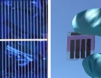
[[File:Imagetheme2.png|thumb|upright=0.9|gauche|link= Photovoltaic materials and devices|[[Photovoltaic materials and devices]]]] |
||
| |
| |
||
[[File: |
[[File:Imagetheme3.png|thumb|upright=0.7|gauche |link= Functional materials and sensors|[[Functional materials and sensors]]]] |
||
|} |
|} |
||
{| |
{| |
||
<big> The |
<big> The team's work is organised into 3 main activities which are described in more detail below: </big> |
||
|} |
|} |
||
| Ligne 37 : | Ligne 37 : | ||
| style="width: 10%; | |
| style="width: 10%; | |
||
<big> |
<big> |
||
*'' |
*''1. [[Materials engineering for electronics]]''<br> |
||
*'' |
*''2. [[Photovoltaic materials and devices]]''<br> |
||
*'' |
*''3. [[Functional materials and sensors]]''<br> |
||
</big> |
</big> |
||
|} |
|} |
||
| Ligne 48 : | Ligne 47 : | ||
'''ICube UMR 7357 - Engineering science, computer science and imaging laboratory '''<br> |
'''ICube UMR 7357 - Engineering science, computer science and imaging laboratory '''<br> |
||
'''D-ESSP department - MaCEPV team ''' |
'''D-ESSP department - MaCEPV team ''' <br> |
||
23, rue du Loess - BP 20 CR - 67037 STRASBOURG Cedex 2 - France <br> |
|||
Tel.: +33 (0)3 88 10 6328 |
|||
© 2013 ICube - Website created by ICube - [[Legal notice]] |
© 2013 ICube - Website created by ICube - [[Legal notice]] |
||
Version du 11 mars 2020 à 11:07
|
Research activities of MaCEPV team |
The activities of the MaCEPV team are at the interface between the physics of electronic materials and the development of elementary semiconductor components. They are based on the team's multidisciplinary skills in the development of thin films by physical or chemical ways, and in the fabrication and advanced characterization of electronic, photovoltaic or optical components.
Our work aims to better understand the physical mechanisms governing the growth of materials in nano-structured thin films, to modify materials by chemical or physical treatments and to study opto-electronic properties that have a strong impact on the functioning of components (electrical conductivity, charge mobility, band structure, absorption and emission spectra, etc.). Materials are generally designed to be integrated as an active element in elementary components in order to improve their "performance" or to provide new functionalities.
The materials studied (since the creation of the team) are, among others, crystalline or microcrystalline silicon, metal oxides based on zinc or tin, nitrides, oxides and oxynitrides, ferroelectric inorganic perovskites, carbon materials such as graphene or Diamond Like Carbon (DLC), or semiconducting polymers and molecular semiconductors. It should be noted that organic materials are developed in close collaboration with several teams of chemists and physico-chemists from local public laboratories.
|
|
ICube UMR 7357 - Engineering science, computer science and imaging laboratory
D-ESSP department - MaCEPV team
23, rue du Loess - BP 20 CR - 67037 STRASBOURG Cedex 2 - France
Tel.: +33 (0)3 88 10 6328
© 2013 ICube - Website created by ICube - Legal notice