« Technologies for inorganic devices » : différence entre les versions
Aller à la navigation
Aller à la recherche
(Created page with "<anyweb> http://www-iness.c-strasbourg.fr/-Technologies-for-inorganic-devices- </anyweb>") |
Aucun résumé des modifications |
||
| Ligne 1 : | Ligne 1 : | ||
[[fr:Technologies pour composants inorganiques]] |
|||
<anyweb> http://www-iness.c-strasbourg.fr/-Technologies-for-inorganic-devices- </anyweb> |
|||
This platform includes equipment designed for studies ranging from fundamental physics to the elaboration of small devices or demonstrators in the field of micro- and nanotechnologies and photovoltaics. |
|||
Specific techniques designed for photovoltaic processes are one of the strategic axes. |
|||
This platform is divided into two sections. |
|||
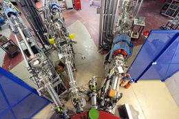
=Ion beam platform= |
|||
[[File:implanteur.jpg|260px|right]] |
|||
The Ion beam platform includes: |
|||
(pages in French) |
|||
*an [[implanter EATON 200 kV]] for the modification of materials |
|||
*an [[accelerator Van de Graaff 4 MV]] for the modification and analysis of materials |
|||
*ion beam analysis equipement |
|||
*[[ion beam analysis simulation softwares]] |
|||
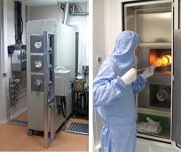
=Clean room platform and peripheral equipment= |
|||
[[File:salleblanche.jpg|260px|right]] |
|||
The fabrication of efficient materials and electronic devices requires complex elaboration and treatment processes. Some steps require a controlled atmosphere, while for some others the fabrication conditions are less critical. Below is more detailed information on: |
|||
(pages in French) |
|||
*[[elaboration and treatment processes]] |
|||
*[[clean room]] |
|||
*[[peripheral equipment]] |
|||
Version du 23 août 2013 à 07:22
This platform includes equipment designed for studies ranging from fundamental physics to the elaboration of small devices or demonstrators in the field of micro- and nanotechnologies and photovoltaics.
Specific techniques designed for photovoltaic processes are one of the strategic axes.
This platform is divided into two sections.
Ion beam platform

The Ion beam platform includes: (pages in French)
- an implanter EATON 200 kV for the modification of materials
- an accelerator Van de Graaff 4 MV for the modification and analysis of materials
- ion beam analysis equipement
- ion beam analysis simulation softwares
Clean room platform and peripheral equipment

The fabrication of efficient materials and electronic devices requires complex elaboration and treatment processes. Some steps require a controlled atmosphere, while for some others the fabrication conditions are less critical. Below is more detailed information on: (pages in French)